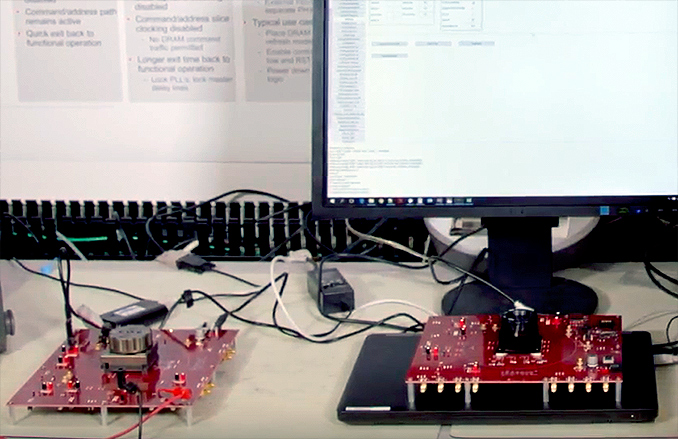
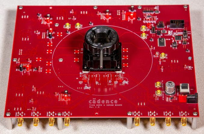
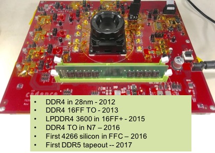
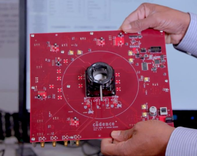
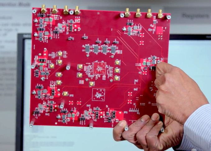
Cadence this week introduced the industry’s first IP interface in silicon for the current provisional DDR5 specification developed by JEDEC. Cadence’s IP and test chip us fabricated using TSMC’s 7 nm process technology, and is designed to enable SoC developers to begin on their DDR5 memory subsystems now and get them to market in 2019-2020, depending on high-volume DDR5 availability. At a special event, Cadence teamed up with Micron to demonstrate their DDR5 DRAM subsystem. In the meantime, Micron has started to sample its preliminary DDR5 chips to interested parties.
DDR5-4400 Initially, DDR5-6400 Eventually
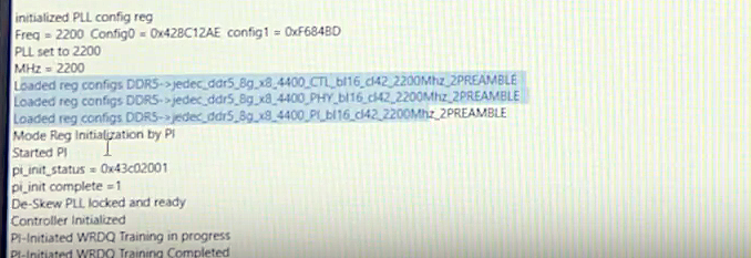
Cadence’s DDR5 memory controller and PHY achieve a 4400 MT/s data rate with CL42 using Micron’s prototype 8 Gb DDR5 memory chips. Compared to DDR4 today, the supply voltage of DDR5 is dropped from 1.2 volts to 1.1 volts, with an allowable fluctuation range of only ±0.033 V. In this case, the specifications mean that an 8 Gb DDR5 DRAM chip can hit a considerably higher I/O speed than an 8 Gb commercial DDR4 IC today at a ~9% lower voltage. JEDEC plans that eventually the DDR5 interface will get to 6400 MT/s, but Cadence says that initial DDR5 memory ICs will support ~4400 MT/s data rates. This will be akin to DDR4 rising from DDR4-2133 at initial launch to DDR4-3200 today. Cadence’s DDR5 demo video can be watched here.
In fact, increased data rates represent only one significant improvement of DDR5 over DDR4. There are several other important features of the upcoming standard: chip capacity, a better channel utilization, integrated voltage regulators, and power management on high-end modules.
Beyond Speed: DDR5 is Primarily About Capacity
There is a great demand for high DRAM capacity from various applications these days, but modern servers can physically accommodate a limited number of memory modules, and contemporary memory controllers can handle a limited number of DIMMs per channel. Therefore, to increase per-machine capacity of DRAM, manufacturers of memory need to build chips of higher capacity. The DDR5 standard enables memory makers to produce 16 Gb and 32 Gb chips by adding internal ECC to boost yields, although memory subsystems will still have to support their own ECC. The new standard also allows for optimizing internal segmentation and optimized timings. In addition to boosting maximum per-die capacity to 32 Gb (we are probably not going to see such DDR5 devices any time soon), JEDEC wants to make vertical stacking easier to simplify building chips based on multi-die chips.
In fact, Marc Greenberg, director of DRAM IP marketing at Cadence, goes as far as saying that:
“DDR5 is mostly a capacity solution, more than performance.”
Modern CPUs and SoCs increase the number of processing cores every year and all of them require memory bandwidth. While DRAM I/O data rates are increasing and the number of memory channels per CPU/SoC is growing, it makes a great sense to increase the utilization of the memory. An improved utilization will increase real world bandwidth available to modern multi-core CPUs/SoCs for servers, storage systems, and other high-performance applications. Using two autonomous buses would be a page from the mobile DRAM playbook — each LPDDR4 device has two independent 16-bit data buses.
DDR5 memory modules will keep using DDR4’s 288-pin arrangement, but because next-gen DDR5 DIMMs will have two separate 32-bit I/O channels, there will be a number of differences when it comes to overall module architecture. First off, DDR5 DIMMs will feature a 16-bit parity signal for ECC (it is logical to expect one 8-bit parity signal for each channel, but this has to be confirmed). Secondly, the channels will have their own Address (Add)/Command (Cmd) buses that will feature a 7-bit width (so, 14 bits in total) and will operate in DDR mode (vs. a single 24-bit bus operating in SDR mode in case of DDR4). It is also important that DDR5 Add/Cmd bus will feature on-die termination to make signals cleaner and to improve stability at high data rates.
Last but not least, high-end DDR5 memory modules for servers will feature their own voltage regulators and power management ICs (PMICs). Because DDR5 chips will feature 16-32 Gb capacities, and their I/O speeds are set to get to 6400 MT/s eventually, they will require a very stable voltage and a very clean power. When it comes to voltage, JEDEC reportedly reduced allowable fluctuation range to 3% (i.e., to ±0.033V), so in order to maintain stability JEDEC wants high-end DDR5 RDIMMs and LRDIMMs to have their own VRMs. As a bonus feature, this will somewhat simplify server motherboards, but the said modules will naturally get more complex and expensive (not that the cost of VRM and PMIC is a problem if you install terabytes of DRAM per box). It is unlikely that consumer DIMMs will also feature their own PMICs and VRMs, although makers of enthusiast-class modules could certainly look into something like this.
First DDR5 Systems Due in 2019–2020
The DDR5 test chip from Cadence was fabricated using TSMC’s latest 7 nm process technology and while Cadence does not specify whether it used TSMC’s CLN7FF (DUV-only) or CLN7FF+ (DUV and EUV) process technology, it does not really matter at present because the processes are largely compatible on the IP level, whereas PHY is not supposed to change (physical interfaces do not really scale).
An important thing about the 7 nm node is that Cadence’s provisional DDR5 IP (the DDR5 controller and PHY) can now be incorporated into SoCs that will be released in 2019-2020, when these process technologies become available to a wide range of TSMC’s customers requiring leading-edge processes featuring maximum transistor density (at this point TSMC’s 7 nm is used by the company’s alpha customers for the node, which are usual suspects — Apple and Qualcomm).
Speaking of commercial availability of SoCs incorporating Cadence’s DDR5 IP, it is noteworthy that Cadence expects the first DDR5-based systems to emerge as early as in 2019. In fact, Cadence seems to be very optimistic about adoption of the new memory type in general.
Cadence: DDR5 to Overtake DDR4 by 2022
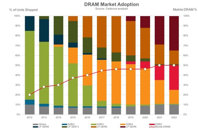
In its blog post about the successful demonstration of a DDR5 memory subsystem, Cadence also touched upon it expectations regarding adoption rate of the new type of DRAM (based on its internal analysis), which are worth looking at.
As noted above, the first systems featuring DDR5 memory are projected to be produced in the next year. These systems will likely be servers running the latest processors due in 2H 2019, or even 2020 (in this case, memory for such machines will be made and procured in 2019). Given the high-scale nature of Intel’s product launches, these servers will likely consume a huge amount of DDR5 chips manufactured by the industry in 2019.
The share of DDR5 chips among all DRAM ICs produced by various makers is predicted to double in 2020 (but still not exceed 10% of all memory chips made that year), based on predictions from Cadence. This probably means that the company does not expect AMD and Intel to release mainstream consumer platforms featuring DDR5 memory that year, so the new DRAM will be used by Xeon and other server-class CPUs/SoCs that year.
Cadence expects adoption of DDR5 to rise significantly in 2021, all the way to around 15%. Meanwhile, in 2022 the adoption of DDR5 will skyrocket to around 25%, whereas adoption of DDR4 will drop to around 15% that year. It is important to note that in 2022 mobile DRAM chips are projected to account for roughly 50% DRAM ICs consumed by the industry, which will likely have an impact on usage of DDR4/DDR5 in higher-end laptops.
It is also noteworthy that Cadence expects “Other” types of DRAM (HBM, GDDR, etc.) to become more widespread in the coming years, possibly because there are plans to use GDDR5 and HBM2 not only for graphics cards, but also for other applications.
DDR5 Final Specification Due This Summer, Start Chip Design Today
The test chip and appropriate IP are ready, Cadence says it can engage with customers who want to start SoC designs with DDR5 memory interfaces. At the same time, Micron can provide samples of chips that comply with preliminary DDR5 spec to interested ecosystem parties.
The final DDR5 specification is expected to be published by JEDEC this summer, which is when makers of DRAM and developers of memory controllers are set to release samples of their products compliant with the actual standard.
Related Reading
- JEDEC: DDR5 to Double Bandwidth Over DDR4, NVDIMM-P Specification Due Next Year
- Micron, Rambus, & Others Team Up To Spur GDDR6 Adoption in Non-GPU Products
- Samsung Updates on GDDR6 Portfolio: 8 Gb and 16 Gb at Multiple Speeds
- Samsung Starts Mass Production of 16Gb GDDR6 Memory ICs with 18 Gbps I/O Speed
- GDDR5X Standard Finalized by JEDEC: New Graphics Memory up to 14 Gbps
- JEDEC Publishes HBM2 Specification as Samsung Begins Mass Production of Chips
Sources: Cadence, Micron, PC Watch
from AnandTech https://ift.tt/2w8zuhk
via IFTTT
No comments:
Post a Comment