Last year we saw the announcement of Cadence’s Tensilica Q6 DSP IP which promised a new architecture that brings integration between vision DSP workloads and new optimised machine learning inferencing workloads. The addition of “AI” capabilities to existing DSP architectures bridges the gap between existing IP blocks such as CPUs or GPUs and more specialised dedicated inferencing IP blocks such as Cadence’s own Tensilica DNA100 block.
Today’s announcement is an evolution of last year’s Q6, further progressing the capabilities we saw introduced in the new architecture and enabling more performance, better density and better power efficiency.
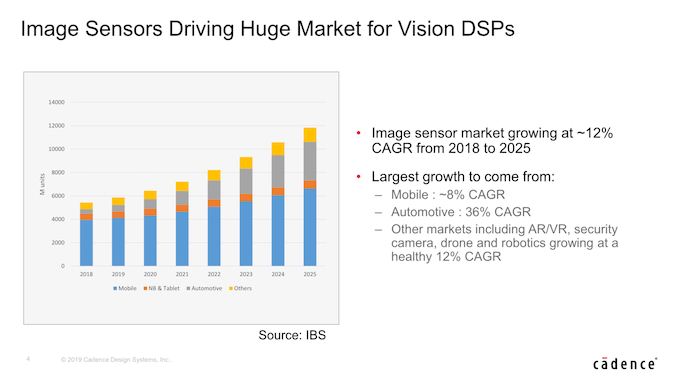
Over the next few years Cadence sees significant growth opportunity for the vision DSP market, with the overall image sensor market growing at a rate of ~12% CAGR till 2025. Naturally those image sensors will need corresponding image processing power behind them in order to transform the raw image data into something meaningful. Particularly the automotive sector is projected to boom enormously in this regard with a continuous annual 36% growth rate, thanks to the projected need for dozens of sensors in future cars.
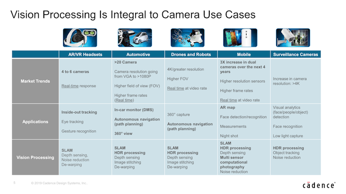
However the growth isn’t solely facilitated by the automotive sector. The mobile and smartphone sector is still projected to be the biggest market, and here growth opportunity is facilitated by the new trend of employing more and more camera modules in smartphones, something that over the last year in particular has become exceedingly evident. Other markets for opportunity are AR/VR headsets which also are projected to require a large numbers of cameras which will need image processing.
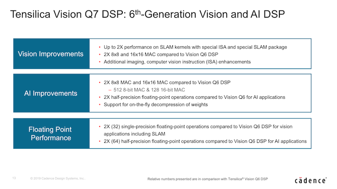
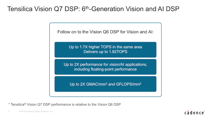
Here’s where the new Tensilica Q7 DSP comes into play. The IP is relatively straightforward in what it brings compared to its predecessor, and that could be summed up as a 2x increase in its performance capabilities.
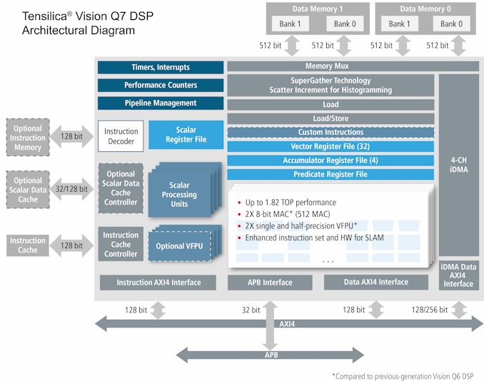
The new architecture has had new ISA instructions for better acceleration of SLAM (Simultaneous Location and Mapping) which is a cornerstone for new AR applications such as Google Lens.
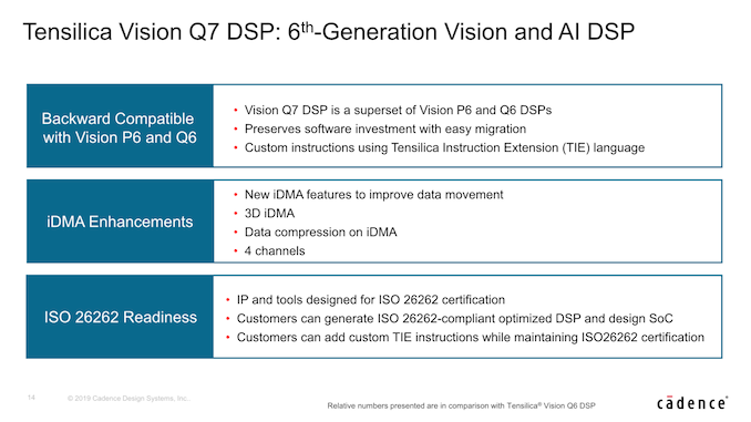
The important aspect of the new IP is that it is fully backwards compatible with existing P6 and Q6 software, which means that vendors who have invested in software do not need to rewrite their algorithms from scratch in order to take advantage of the new performance boosts.
Alongside other improvements in the iDMA of the architecture, such as improved bandwidth enabled through microarchitectural changes and data compression, Cadence put emphasis on ISO26262 requirements which dictate functional safety standards for road vehicles – a must have if the IP is to be employed in the automotive sector.
As mentioned, Cadence has doubled up on the processing units compared to the Q6, resulting in a new a new 512 8-bit MAC engine as well as doubling up the floating point capabilities. Cadence quotes a peak performance of 1.82 TOPs in 8-bit operations, which would result in a frequency of around 1.77GHz which is a natural progression from the peak 1.5GHz we were presented last year with the Q6.
One of the most interesting aspects of the new IP is how Cadence was able to achieve all this and what it means for the area and power efficiency of the block. In fact, Cadence doesn’t expect the new generation to be any bigger than the Q6, and the increase in performance and introduction of more execution units came at very little area cost. Cadence was able to optimise the microarchitecture as such that the new Q7 promises a doubling of GMAC and GFLOPs per mm², which is quite the feat for any IP vendor. Power efficiency gains are also in line with the performance gains, and the company expects a similar 1.7x increase in perf/W.
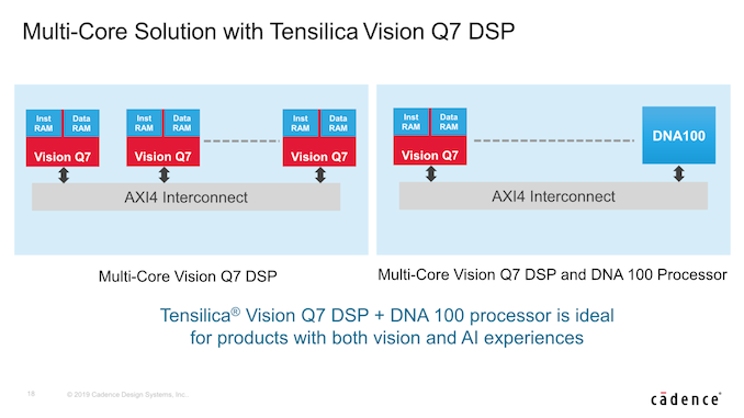
Cadence envisions customers to be able to lay out multiple Q7 blocks alongside each other for performance scaling, and naturally the IP would also be a great fit to put alongside the DNA 100 neural network processor.
Overall, the new IP is a fairly straightforward progression from its predecessor, with a focus on improving the important PPA metrics of the architecture. The IP is said to be ready for general licensing availability in Q2 (this quarter).
Related Reading:
- Cadence Announces Tensilica Vision Q6 DSP
- Cadence Announces The Tensilica DNA 100 IP: Bigger Artificial Intelligence
- Cadence Tapes Out GDDR6 IP on Samsung 7LPP Using EUV
- Cadence & Micron DDR5 Update: 16 Gb Chips on Track for 2019
- Cadence and Micron Demo DDR5-4400 IMC and Memory, Due in 2019
from AnandTech http://bit.ly/2WGl6FW
via IFTTT
No comments:
Post a Comment