Thursday, 26 July 2018

We Test a $1,000 CPU From 2010 vs. Ryzen 3

https://ift.tt/2LTRRdr


Today we're going to have a bit of benchmark fun as we test out a processor we reviewed in 2010. The Core i7-980X was a hexacore beast, but how does it stack up 8 years later? To find out I'm going to compare it with a whole heap of modern...

Read Entire ArticleRead Comments


from TechSpot https://ift.tt/2LnAuoW
via IFTTT

Microsemi Announces SmartRAID Cards With On-Board Supercapacitors And Encryption

https://ift.tt/2LspZAZ

Last year, Microsemi released a new generation of 12Gbps SAS controller chips, then incorporated them into a variety of SAS/SATA host bus adapter (HBA) and RAID cards under their Adaptec brand. Now, their SmartRAID family of advanced RAID cards is getting two new models that bring new features to the product line.

First up is the SmartRAID 3162-8i, which decodes to indicate a card with 8 internal ports and a 2GB DRAM cache with power loss protection. This is the first Adaptec RAID card to feature a fully-integrated power loss protection scheme including supercapacitors on the card itself. Previous SmartRAID cards such as the 3152-8i have all required an external supercapacitor module to be mounted in another expansion slot or elsewhere in the server. Putting supercapacitors on the half-height half-length card makes it fairly crowded and has the potential to restrict air flow across the controller, so Microsemi has upgraded many components on the card with industrial-grade parts rated for higher temperatures. This has also allowed Microsemi to spec the card for 150 linear feet per minute (LFM) of airflow instead of the 200 LFM required by the 3152-8i and similar cards.

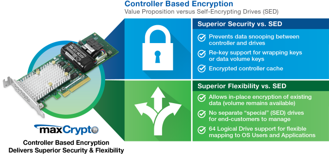
The second new product is the SmartRAID 3162-8i/e, which uses the same hardware as above but is the first SmartRAID card to enable the encryption capabilities of the SmartROC 3100 controller chip. This controller-based encryption offers an alternative to using self-encrypting drives (SEDs) or software encryption on the host CPU. Microsemi brands this encryption system as maxCrypto, and touts its combination of the minimal performance overhead of SEDs with the flexibility of software encryption to support things like a mix of encrypted and unencrypted volumes, and re-keying or re-encrypting existing data in-place.

The encryption keys are derived using a master passphrase that generates a master key stored on the controller card. Each encrypted RAID volume created on the controller gets a separate volume encryption key generated by the master key. In the event that the RAID card dies, a replacement card can be swapped in and can reconstruct all the volume keys using the original master passphrase. The cipher used us AES256 in XTS mode.

The new cards are in volume production now.


from AnandTech https://ift.tt/2JXOC2G
via IFTTT

Intel's 8-core i9 9900K and i7 9700K are reportedly soldered

https://ift.tt/eA8V8J

The first soldered mainstream CPU since Sandy Bridge

from Overclock3D.Net https://ift.tt/2LB90eJ
via IFTTT

Wednesday, 25 July 2018

Intel’s Xeon Scalable Roadmap Leaks: Cooper Lake-SP, Ice Lake-SP Due in 2020

https://ift.tt/2mJJkyM

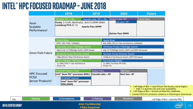
Recently a Chinese university has published a collection of slide-decks from various companies covering a server/HPC event. Among the slides, Intel had a seemingly longer comprehensive presentation describing Intel’s conceptual approaches to HPC to analysis of various workloads, and most interestingly, future plans and what looks to be an up-to-date server roadmap.

According to slides published by the Central South University from Changsha City, Hunan, Intel had to delay its Ice Lake-SP server platform from 2019 to 2020 because of the general delay of its 10 nm process technology. What was unknown and newly revealed in the roadmap, is that in addition to the codenamed Ice Lake-SP processors, the company is also preparing the codenamed Cooper Lake-SP CPUs that are set to arrive a bit ahead of the Ice Lake-SP chips. The document was demonstrated to students and professors by Intel itself at a special server/HPC event earlier this month.

Both Cooper Lake-SP and Ice Lake-SP processors will support the codenamed Barlow Pass DIMMs, which is most probably Intel’s next-generation Optane DC Persistent Memory DIMM running next-gen 3D XPoint non-volatile memory (though it is a speculation at this point). Intel does not disclose the difference between the Cooper Lake-SP and the Ice Lake-SP products, but it is possible that the former is the company’s “Plan B” for next-generation servers should anything happen with its 10 nm process technology or the ICL-SP design. Meanwhile, both Cooper Lake-SP and Ice Lake-SP will belong to one server platform that will also support an eight-channel per-socket memory sub-system along with multiple OmniPath fabric innovations.

Intel expects to begin production ramp of its Cooper Lake-SP CPUs in late 2019 or early 2020 with end user availability in late Q1 2020 or mid-2020. By contrast, the Ice Lake-SP will start their ramp sometimes in late Q1 2020 and will be available in Q3 or Q4 of 2020.

Another interesting thing to point out in Intel’s roadmap is that the company is prepping the codenamed Walker Pass platform and the codenamed Cascade Lake-AP processor for the HPC market segment. The aforementioned CPU is said to replace the Xeon Phi 7200-series “Knights Landing” processor for technical computing. Meanwhile, as the name suggests, the Cascade Lake-AP will heavily rely on Skylake SP-based design for mainstream servers.

Intel traditionally does not comment on information obtained unofficially and therefore we cannot find out how accurate the current roadmap is.

Related Reading:

Via: Twitter / David Shor


from AnandTech https://ift.tt/2NHRX8g
via IFTTT

Intel Provides Royalty-Free License for Data Bus to DARPA’s Modular Chips Initiative

https://ift.tt/2LCYpQx

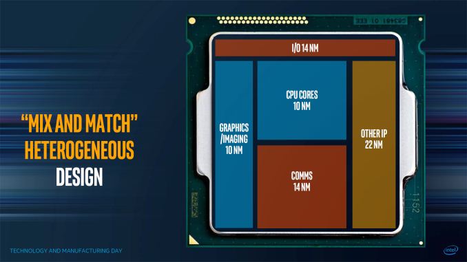
Taking place this week is DARPA’s 2018 Electronic Resurgence Initiative (ERI) Summit, the defense research agency's first gathering to address the direction of US technology manufacturing as Moore's Law slows down, and how the agency can jumpstart alternative efforts to ensure continued performance scaling. To that end, in an interesting and unexpected move from the summit, Intel has announced that it would offer a royalty-free license for its Advanced Interface Bus (AIB) to participants of the agency’s Common Heterogeneous Integration and Intellectual Property (IP) Reuse Strategies (CHIPS) program. The move will help interested parties to design SoCs utilising heterogeneous components made using different process technologies.

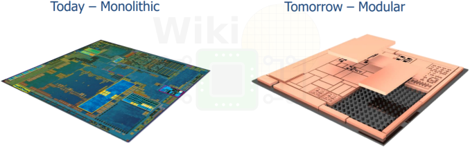
Modern, complex chips are hard to manufacture and equally hard to design, as they frequently contain a number of different application-specific functional blocks (e.g., general-purpose cores, graphics cores, etc.). In a bid to somehow reduce costs of chip design, numerous companies have come up with modular development approaches that allow them to design SoCs using more or less standard components. This methodology is used to develop modern SoCs for mobiles, game consoles, and other consumer electronics. However, it is largely believed that the approach is still not enough cost-effective for future SoCs, as the entire chip must still be manufactured as a single, monolithic die. As a result, Intel has propose using so-called chiplets, which are heterogeneous components of a chip produced using different process technologies and interconnected using its AIB interface.

Intel’s Advanced Interface Bus is a low-power die-to-die interface that is based on a forward clock parallel I/O architecture. AIB features a 1 Gbps per lane SDR transfer rate for control signals and a 2 Gbps per lane DDR transer for data. AIB is agnostic to particular packaging technology used: it can rely on Intel’s own EMIB, or can use other packaging technologies (e.g., CoWoS, InFO, etc.) too. Intel itself of course uses its AIB for its Stratix 10 FPGAs (more on this here), but since the tech is universal, participants of the CHIPS program will be able to use the interface for whatever projects they are working on.

The whole idea behind the CHIPS initiative is to enable developers of SoCs to re-use existing semiconductor blocks for future projects, and to only build blocks on the smallest/most powerful (read: expensive) manufacturing process that part requires. Intel itself proposes to use 10-nm CPU and GPU cores along with communication blocks produced using a 14 nm fabrication process, as well as other components made using a 22 nm manufacturing tech. For developers who do not have access for Intel’s technologies and who have considerably lower R&D budgets, it will make sense to re-use some of the IP produced using a planar fabrication process with processing cores made using a leading-edge FinFET technology.

It remains to be seen when participants of DARPA’s CHIPS program actually start to use Intel’s AIB, but the fact that they now have a technology that could wed leading-edge IP with proven blocks looks rather promising.

Related Reading:


from AnandTech https://ift.tt/2LmR9ZO
via IFTTT

Synology 2018 NAS and Wi-Fi Lineup Sneak Peek

https://ift.tt/2NGqBQ4

Yesterday we published an interview with Alex Wang, CEO of Synology America, and as part of that interview we were able to get a sneak peak into some of the new NAS and Wi-Fi products that Synology is planning to launch through to the end of 2018.

Wi-Fi

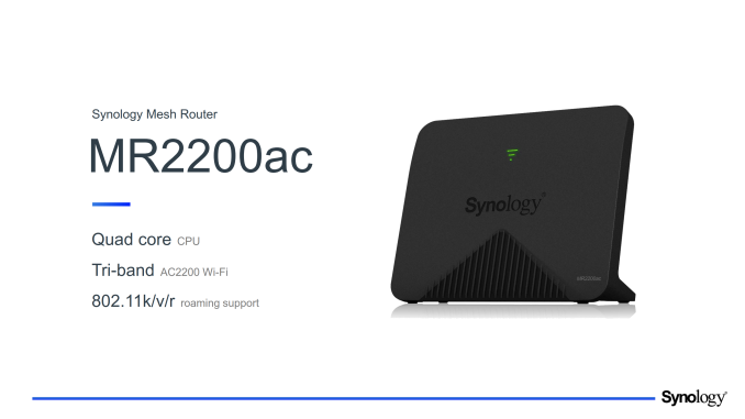
The company plans to introduce a follow-up to the RT2600ac released earlier this year. The new MR2200ac comes with mesh features. Similar to other mesh routers from the top tier vendors, the MR2200ac sports the Qualcomm IPQ4019 SoC with integrated dual-band Wi-Fi. The additional PCIe interface enables Synology to add a second 5 GHz radio, turning the MR2200ac into a tri-band router. Like the Netgear Orbi, the MR2200ac plans to use the second 5 GHz radio for backhaul purposes. Synology has built up on Qualcomm's Wi-Fi SON features to enable the MR2200ac to mesh with the RT2600ac (also Qualcomm-based). The RT1900ac, unfortunately, will not be compatible for meshing purposes. Synology is planning to bring in features such as easy parental control and threat prevention (antivirus / malware scanning etc.) to make their routers stand out in the crowded market.
Business

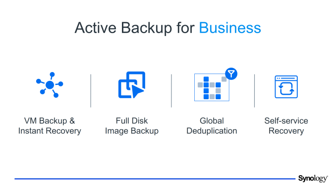
In terms of subscription-based value additions for business users, Synology is launching Active Backup for Office 365 as part of their Active Backup suite. The Active Backup for Business service includes backup of virtual machines, instant recovery, full disk image backups with dedupe etc.
Storage

Being primarily focused on storage solutions, Synology will naturally offer several new NAS aimed at customers with different requirements later this year. In total there will be four new NAS products: two in a desktop form-factor and two in a rackmount form-factor. All four machines will support Synology’s typical NAS software with well-known capabilities.

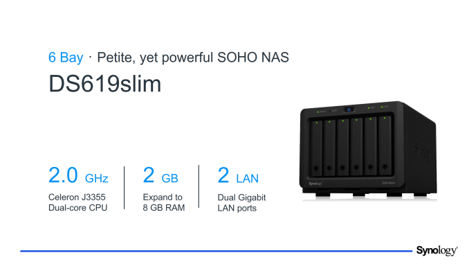
  • DS619slim using an Intel Celeron J3355 and sporting 6x 2.5" drive bays
  • DS2419+ using the Intel C3538 Denverton processor and providing 12 bays in a desktop form factor.
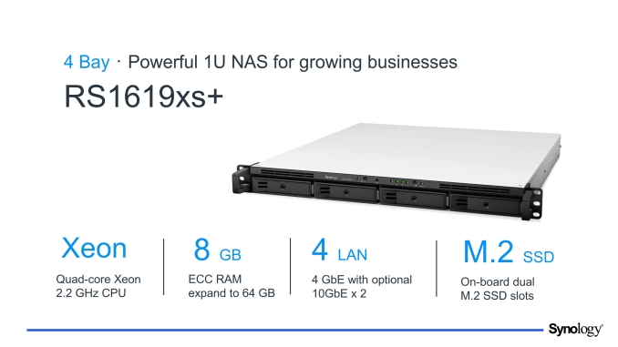
  • RS1619xs+ using a Xeon CPU in a 1U form-factor and providing 4 bays
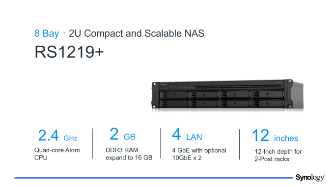
  • RS1219+ using the older Rangeley family CPU with 8 bays in a short-depth 2U form factor

The most basic of Synology’s upcoming NAS devices is the DS619slim aimed at small office/home office markets. The DS619slim is based on Intel’s dual-core Celeron J3355 SoC (Apollo Lake) outfitted with 2 GB – 8 GB of RAM. The NAS has six 2.5-inch bays for HDDs or SSDs, but it does not look that it supports caching on an SSD for additional performance (at least today’s entry-level NAS products from Synology do not support this feature). Meanwhile, since RAID stripe mode will be supported, we are still talking about read/write performance of about ~500 MB/s even with hard drives. As for network connectivity, the DS619slim will have two GbE ports.
A more powerful NAS that Synology will have later this year is the DS2419+. This NAS is powered by Intel’s quad-core Atom C3538 SoC (Denverton), is equipped with 4 – 32 GB of RAM as well as four GbE network connectors. The DS2419+ will have 12 bays and will support a PCIe slot for a caching M.2 SSD or a 10 GbE NIC.

Moving on to rackmount NAS for businesses that require a higher performance and/or more storage space. First up is the 1U RS1619xs+ NAS based on Intel’s quad-core Xeon processor clocked at 2.2 GHz and equipped with 8 – 64 GB of DDR4 memory with ECC. This NAS has four bays and two M.2. SSD slots for high-performance caching drives. By default, the RS1619xs+ will be equipped with four GbE LAN ports, but optionally Synology may install two 10 GbE NICs for those who have appropriate networks.
For customers who need a higher capacity, Synology will offer its 2U RS1219+ NAS featuring eight bays and powered by Intel’s quad-core Atom SoC and 2 – 16 GB of DDR3 memory. The machine will feature 4 GbE controllers by default or two optional 10 GbE ports for those who can use them.
Pricing of the new NAS units will be announced when Synology starts to offer them commercially.

Synology's NAS Due in 2H 2018
  DS619slim DS2419+ RS1619xs+ RS1219+
Form-Factor Desktop 1U 2U
SoC Dual-Core
Celeron J3355
Quad-Core
Atom C3538
Quad-Core Xeon Quad-Core Atom
RAM 2 - 8 GB 4 - 32 GB 8 - 64 GB 2 - 16 GB
Number of Bays 6 12 4 8
Caching SSDs - M.2/NVMe
(or 10GbE)
2 × M.2 NVMe SSDs ?
Network Connectivity 2 × GbE 4 × GbE
or 1 × 10 GbE
4 × GbE
or 2 × 10 GbE

Related Reading


from AnandTech https://ift.tt/2LjVSvj
via IFTTT

Intel Officially Launches Bean Canyon NUCs with Coffee Lake-U Processors

https://ift.tt/2LoTLqb

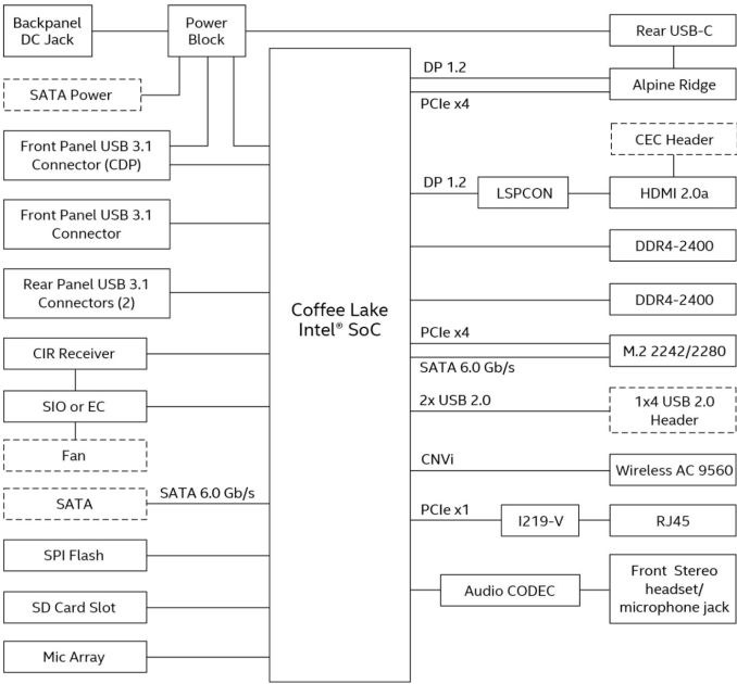
Intel's Bean Canyon NUCs have been subject to a number of leaks, notably from FanlessTech. However Intel has finally made things official with a detailed technical product manual for all the members of the Bean Canyon NUC family. From an I/O perspective, the Bean Canyon NUCs look very similar to the Baby Canyon NUCs. However, the internals have gone in for a significant revamp, thanks to the Coffee Lake processors (CFL-U) inside. The updates include:

  • 28W TDP processors across all SKUs, with true quad-core / octa-thread options
  • Iris Plus Graphics 655 with 128MB eDRAM across all SKUs
  • Intel Wireless-AC 9560 with Bluetooth 5.0 WLAN module
  • USB 3.1 Gen 2 (10 Gbps) support on all external Type-A ports

While most of the Baby Canyon NUCs came with a 15W TDP processor - either in a "2+2" or "2+3e" configuration - all the Bean Canyon models (NUC8BE) sport 28W TDP processors (that can be configured to run with a lower TDP of 20W, if needed). The 28W TDP allows all the models to come with Iris Plus Graphics 655 with 128MB of eDRAM as the integrated GPU. This makes "2+3e" CPUs the new baseline, while even more powerful "4+3e" CPUs are now an option.

Since these are U-series processors, the PCH is on-package with the rest of the CPU. The move to the Cannon Point-LP integrated PCH allows for four USB 3.1 Gen 2 ports that are present as Type-A ports in the front and rear of the chassis. The CFL-U come with the new Integrated Connectivity feature (CNVi), where the Wi-Fi and Bluetooth MAC and other functional blocks are put inside the processor. The CRF (companion RF) module completes the Wireless-AC 9560 by implementing the signal processing, RF, and analog functions.

The Intel Wireless-AC 9560 is a significant upgrade over the Wireless-AC 8265 in the Kaby Lake NUCs. It comes with Wave 2 features, including support for 160 MHz channels and downlink MU-MIMO. The 2x2 WLAN module is theoretically capable of 1.73 Gbps bandwidth. It also integrates dual-mode Bluetooth 5 support.

Intel Bean Canyon NUC PCs (Non-Optane SKUs)
  NUC8i7BEH NUC8i5BEH NUC8i5BEK NUC8i3BEH NUC8i3BEK
CPU Core i7-8559U
4C/8T
2.7 (4.5) GHz
28 W TDP
Core i5-8259U
4C/8T
2.3 (3.8) GHz
28 W TDP
Core i3-8109U
2C/4T
3.0 (3.6) GHz
28 W TDP
Graphics Intel Iris Plus Graphics 655
PCH Intel Cannon Point-LP for Coffee Lake-U
Memory Two SO-DIMM slots, up to 32 GB of DDR4-2400
2.5" bay 1x2.5"/9.5mm bay, SATA3 None 1x2.5"/9.5 mm bay, SATA3 None
M.2 Slot Up to M.2-2280 SSD with SATA3 or PCIe 3.0 x4 interface
Wi-Fi/BT Soldered-down Intel Wireless-AC 9560(802.11ac 2x2 + BT 5.0) with WiDi support
Ethernet Intel I219V Gigabit Ethernet controller
Display Outputs DisplayPort 1.2 via USB-C connector
HDMI 2.0
Audio 3.5 mm TRRS audio jack
7.1 channel audio output via HDMI or DP
Thunderbolt
& USB-C
1x Thunderbolt 3 Type-C (40 Gbps) (USB 3.1 Gen 2 and Display Port functionality included)
USB 4 USB 3.1 Gen 2 Type-A (10 Gbps), one with charging
Other I/O MicroSDXC card reader with UHS-I support
One infrared receiver
Size (mm) 115 × 111 × 51 115 × 111 × 31 115 × 111 × 51 115 × 111 × 31
PSU External, 65 W

Intel continues to use a LSPCon on board to convert the Display Port 1.2 output of the processor to a HDMI 2.0 port with HDCP 2.2. Unfortunately, stereoscopic 3D will not be supported. The good news is that the Thunderbolt 3 USB Type-C port on all the models will also support 4Kp60 displays with HDCP 2.2. All versions of the Bean Canyon will support Thunderbolt 3 (unlike the Core i3 version of the KBL-U Baby Canyon that restricted the Alpine Ridge Type-C port to USB 3.1 Gen 2 only in the firmware).

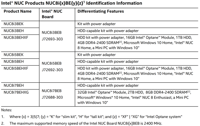
Similar to the previous NUCs, Intel plans to sell both kit (NUC8iXBEK / NUC8iXBEH) and board versions (NUC8iXBEB) of the different configurations. Note that the BEK does not support a 2.5" drive, while the BEH SKUs do. System builders using the BEB SKUs can opt to operate the processor in the cTDP down (20W) mode if adequate cooling is not available. Intel also plans to offer pre-built systems with Optane, as described below.

Retail availability is expected to be in early August. Pricing details are yet to be made available.


from AnandTech https://ift.tt/2JPXUxH
via IFTTT
Related Posts Plugin for WordPress, Blogger...