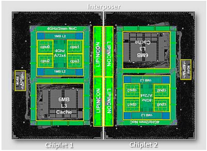
Arm and TSMC this week unveiled their jointly developed proof-of-concept chip that combines two quad-core Cortex-72-based 7 nm chiplets on TSMC’s Chip-on-Wafer-on-Substrate (CoWoS) interposer. The two chips are connected using the company’s Low-voltage-IN-Package-INterCONnect (LIPINCON) interface. The chip is meant to showcase potential of Arm’s and TSMC’s technologies for high-performance computing applications.
Large SoCs are hard and expensive to manufacture with decent yields using leading-edge process technologies these days. In fact, many elements of these SoCs do not need to be produced using the latest nodes at all. As a result, many chipmakers turn to the so-called chiplet design approach that relies on multiple smaller dies optimized for a particular function and produced using an appropriate process technology. Smaller dies afford better yields and better binning, allowing for a quicker return on investment. These smaller dies need to communicate with each other using a high-bandwidth low-latency and low-power inter-chiplet connections and the latter are the corner stone of any chiplet design.
The proof-of-concept system contains two chiplets made using TSMC’s N7 process technology and placed on a CoWoS interposer. Each chiplet features four Arm Cortex-A72 cores running at a whopping 4 GHz (this core was designed to run at <2 GHz frequencies inside mobile SoCs) that are interconnected using an on-die network-on-chip (NoC) mesh bus operating at 4 GHz. The cores are equipped with a 2 MB L2 cache (512 KB per core) as well as a 6 MB unified L3 cache.
The two chips are connected to each other using a LIPINCON die-to-die inter-chiplet connection that operates at 8 GT/s data transfer rate at 0.3 V and offers 320 GB/s bandwidth. When it comes to overall efficiency of LIPINCON on CoWoS, TSMC says that it features a 0.56 pJ/bit (pico-Joules per bit) power efficiency as well as a 1.6 Tb/s/mm2 (terabits per second per square millimeter) bandwidth density.
The proof-of-concept chiplet system was taped out in December 2018, and made in April 2019, so both Arm and TSMC had plenty of time to play with it. The chip will never be sold in volume, but it proves that technologies by the two companies can enable designers to build complex chiplet-based products with unique characteristics. THe companies are hoping that now this technology is proven that its customers will take advantage of it.
Related Reading:
- Hot Chips 31 Keynote Day 2: Dr. Phillip Wong, VP Research at TSMC (1:45pm PT)
- TSMC Announces Performance-Enhanced 7nm & 5nm Process Technologies
- TSMC: First 7nm EUV Chips Taped Out, 5nm Risk Production in Q2 2019
- TSMC Kicks Off Volume Production of 7nm Chips
Source: TSMC
from AnandTech https://ift.tt/2mmvfuq
via IFTTT

No comments:
Post a Comment