One of the measures of how quickly a new process node gains traction is by comparing how many wafers are in production, especially as that new process node goes through risk production and then into high volume manufacturing. You can tell a lot about how much confidence a foundry has in its new process by looking at the number of wafers in production, as well as the expected range of customers and products that are set to be produced. As part of TSMC’s Technology Symposium 2020, we were treated to a little insight into the growth of its new 5nm process technology.
TSMC’s 5nm process, or strictly speaking its first production version of 5nm, known as N5, is currently in the process of high volume manufacturing. We are expecting the first consumer products that use N5 processors, particularly smartphones, out by the end of the year. That means that the companies who are building those products have already worked with pre-production silicon for validation, put their orders in for N5 parts, and may already be getting the first deliveries of the new hardware.
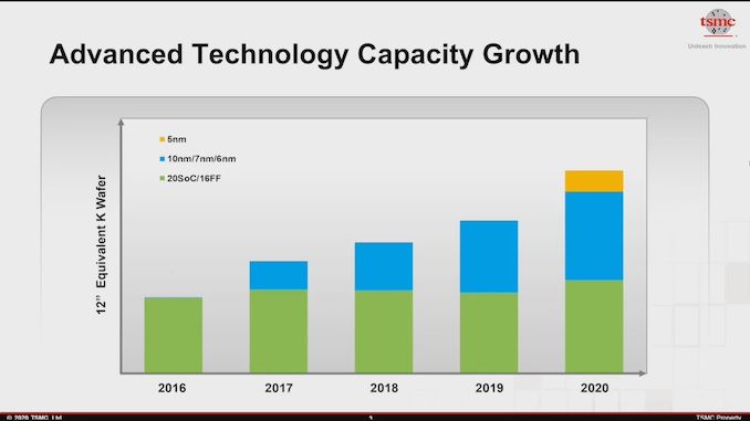
With such a new process, we always expect that initial production, even in ‘high volume production’ mode, is usually slow. This is due to product development, but also extensive validation and to make sure that the product isn’t a dud (such as TSMC’s ill-fated 20nm process). However, judging by the slides produced by TSMC at its Technology Symposium, it looks like that 11% of its 2020 production of 16nm+ wafers will be on 5nm.
It should be noted that this graph has ’12-inch wafer equivalents’ as the y-axis, which means that if any process node would use 8-inch wafers, it would be scaled accordingly. However, all of these leading edge process nodes are likely to be on 12-inch wafers.
Unfortunately there’s no real sense of how many wafers that is. TSMC has stated in another slide that it produced over 12 million 12-inch wafer equivalents in 2019, but that covers all processes and all facilities. At financial disclosures, TSMC does a breakdown of each node, but only in terms of revenue.
However, comparing 5nm to TSMC’s 7nm capability, it does show that 2019 to 2020, 7nm increased by 22.7%, and in 2020, 5nm production will be ~24% of 7nm production. This leads into TSMC’s narrative that it expects to grow its 5nm production to double in 2021, and triple in 2022, using the 2020 numbers as a base.
TSMC did give some insight into its 5nm manufacturing facilities also.
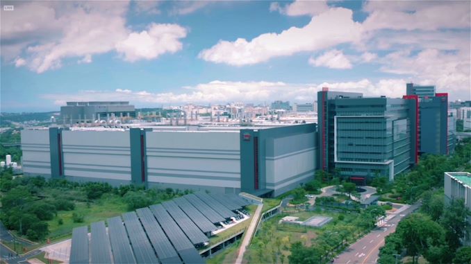
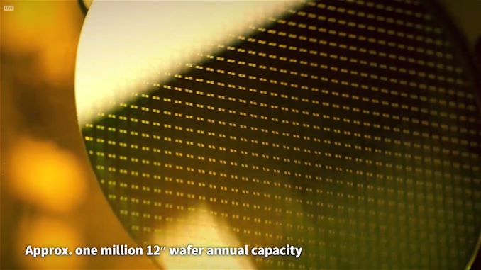
All of TSMC’s 5nm chips are being built at TSMC’s Fab 18, the newest fabrication plant that spreads over six buildings, which TSMC calls its ‘fourth GigaFab’. Fab 18 broke ground on January 26th 2018, and a year later the company started installing over 1300 manufacturing tools, including EUV machines, in a process that only took 8 months. From there, the company started testing its 5nm risk production, and started high-volume manufacturing in Q2. TSMC states that Fab 18 is capable of producing over one million 12-inch wafers per year, all on 5nm, and claims it leads the industry in energy efficiency for a fab of it size.
Related Reading
- TSMC Details 3nm Process Technology: Full Node Scaling for 2H22 Volume Production
- TSMC To Build 5nm Fab In Arizona, Set To Come Online In 2024
- TSMC & Broadcom Develop 1,700 mm2 CoWoS Interposer: 2X Larger Than Reticles
- TSMC Boosts CapEx by $1 Billion, Expects N5 Node to Be Major Success
- Early TSMC 5nm Test Chip Yields 80%, HVM Coming in H1 2020
- TSMC: 5nm on Track for Q2 2020 HVM, Will Ramp Faster Than 7nm
- TSMC: N7+ EUV Process Technology in High Volume, 6nm (N6) Coming Soon
from AnandTech https://ift.tt/3lhiydZ
via IFTTT


No comments:
Post a Comment