One of the main drivers for the semiconductor industry is the growth in always-connected devices that require silicon inside, either for compute, communication, or control. The ‘Internet of Things’ era, depending on who you speak to, is set to scale to many billions of devices and subsequently many billions of dollars in opportunities. In order to drive this segment, semiconductor foundries have been developing cost-effective low power process node technologies for its customers to help drive a new level of power efficiency and low cost implementations. TSMC’s newest process targeting this market was announced at its 2020 Technology Symposium, and is to be called N12e.
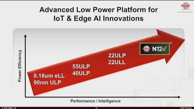
TSMC’s roadmap for its low powered platforms has centered around popular process node technologies optimized for low power and low leakage. Over the past decade TSMC has offered low power versions of 90nm, 55nm, 40nm and 22nm, with each generation giving smaller die areas and lower power, as well as other design optimizations specific to each need. These have all been planar technologies, however the new N12e process node is the next generation, and based on FinFETs.
FinFETs are, in a like-for-like scenario, more complex to build than planar transistors, and therefore should naturally cost more to produce. However, FinFET technologies also provide benefits in scaling and power, something this market is interested in. Rather than introduce FinFETs earlier in the cycle, TSMC has waited a few generations until it can deploy its most advanced FinFET designs to this market, to help ease the transition with the benefits that a most optimized design could bring.
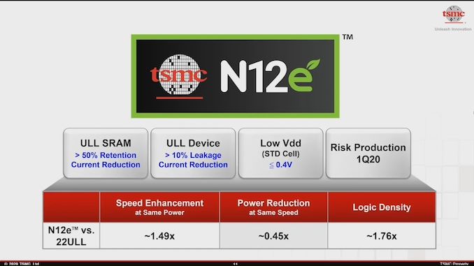
Within N12e compared to 22ULL, TSMC is promising a 1.49x increase in frequency at iso-power, or a 55% reduction in power at iso-speed. This also comes with a 1.76x increase in logic density, and a specialist low-voltage cell library capable of 0.4 volts. This extends the range of TSMC’s IoT process node offerings to a lower power bracket, as well as giving a better performance profile at all other powers as well.
N12e brings together technology from TSMC’s 16nm process and couples it with improvements and experience from 12FFC+, both of which have been used extensively in high performance computing. TSMC believes that integrating this with its ultra-low-leakage knowledge will help enable the next generation of 5G-enabled IoT Edge devices, by providing low power routes to AI accelerators for speech recognition, health monitoring and machine vision.
The main competitor to N12e would be GlobalFoundries 12FDX platform, which is built on GF’s 12nm FD-SOI technology, with claims of better power consumption and lower cost than equivalent FinFET designs. However despite talk of 12 FDX for several years (and news of new MRAM support and such), there have been no public design wins for the process.
It is unclear when TSMC will start taking orders for its N12e platform, however the company has said it is ‘excited’ for the next generation of products built on it.
Source: TSMC N12e
Related Reading
- TSMC Details 3nm Process Technology: Full Node Scaling for 2H22 Volume Production
- TSMC To Build 5nm Fab In Arizona, Set To Come Online In 2024
- TSMC & Broadcom Develop 1,700 mm2 CoWoS Interposer: 2X Larger Than Reticles
- TSMC Boosts CapEx by $1 Billion, Expects N5 Node to Be Major Success
- Early TSMC 5nm Test Chip Yields 80%, HVM Coming in H1 2020
- TSMC: 5nm on Track for Q2 2020 HVM, Will Ramp Faster Than 7nm
- TSMC: N7+ EUV Process Technology in High Volume, 6nm (N6) Coming Soon
- GlobalFoundries' 22FDX with MRAM is Ready
- GlobalFoundries Announces 22FDX Milestone: $2 Billion in Design Wins
from AnandTech https://ift.tt/3lonM7Q
via IFTTT


No comments:
Post a Comment