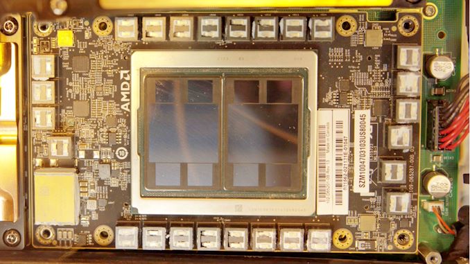
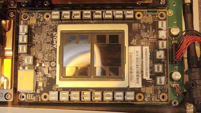
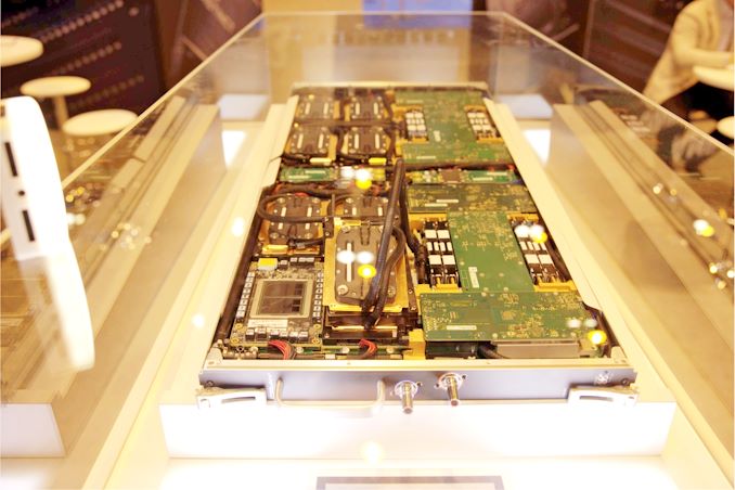
One of the big announcements at AMD’s Data Center event a couple of weeks ago was the announcement of its CDNA2 based compute accelerator, the Instinct MI250X. The MI250X uses two MI200 Graphics Compute Dies on TSMC’s N6 manufacturing node, along with four HBM2E modules per die, using a new ‘2.5D’ packaging design that uses a bridge between the die and the substrate for high performance and low power connectivity. This is the GPU going into Frontier, one of the US Exascale systems due for power on very shortly. At the Supercomputing conference this week, HPE, under the HPE Cray brand, had one of those blades on display, along with a full frontal die shot of the MI250X. Many thanks to Patrick Kennedy from ServeTheHome for sharing these images and giving us permission to republish them.
The MI250X chip is a shimmed package in an OAM form factor. OAM stands for OCP Accelerator Module, which was developed by the Open Compute Project (OCP) – an industry standards body for servers and performance computing. And this is the accelerator form factor standard the partners use, especially when you pack a lot of these into a system. Eight of them, to be exact.
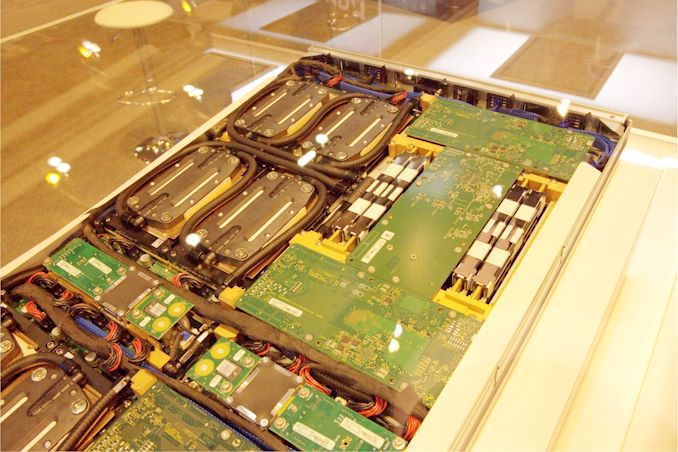
This is a 1U half-blade, featuring two nodes. Each node is an AMD EPYC ‘Trento’ CPU (that’s a custom IO version of Milan using the Infinity Fabric) paired with four MI250X accelerators. Everything is liquid cooled. AMD said that the MI250X can go up to 560 W per accelerator, so eight of those plus two CPUs could mean this unit requires 5 kilowatts of power and cooling. If this is only a half-blade, then we’re talking some serious compute and power density here.
Each node seems relatively self-contained – the CPU on the right here isn’t upside down given the socket rear pin outs aren’t visible, but that’s liquid cooled as well. What looks like four copper heatpipes, two on each side of the CPU, is actually a full 8-channel memory configuration. These servers don’t have power supplies, but they get the power from a unified back-plane in the rack.
The back connectors look something like this. Each rack of Frontier nodes will be using HPE’s Slingshot interconnect fabric to scale out across the whole supercomputer.
Systems like this are undoubtedly over-engineered for the sake of sustained reliability – that’s why we have as much cooling as you can get, enough power phases for a 560 W accelerator, and even with this image, you can see those base motherboards the OAM connects into are easily 16 layers, if not 20 or 24. For reference, a budget consumer motherboard today might only have four layers, while enthusiast motherboards have 8 or 10, sometimes 12 for HEDT.
In the global press briefing, Keynote Chair and Professor world renowned HPC Professor Jack Dongarra, suggested that Frontier is very close to being powered up to be one of the first exascale systems in the US. He didn’t outright say it would beat the Aurora supercomputer (Sapphire Rapids + Ponte Vecchio) to the title of first, as he doesn’t have the same insight into that system, but he sounded hopeful that Frontier would submit a 1+ ExaFLOP score to the TOP500 list in June 2021.
Many thanks to Patrick Kennedy and ServeTheHome for permission to share his images.
from AnandTech https://ift.tt/3kO2UrV
via IFTTT


No comments:
Post a Comment