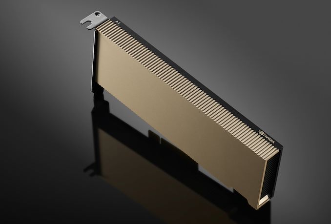
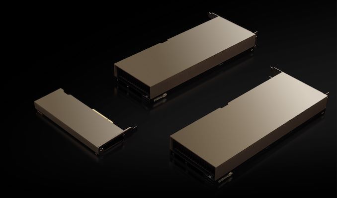
Alongside a slew of software-related announcements this morning from NVIDIA as part of their fall GTC, the company has also quietly announced a new server GPU product for the accelerator market: the NVIDIA A2. The new low-end member of the Ampere-based A-series accelerator family is designed for entry-level inference tasks, and thanks to its relatively small size and low power consumption, is also being aimed at edge computing scenarios as well.
Along with serving as the low-end entry point into NVIDIA’s GPU accelerator product stack, the A2 seems intended to largely replace what was the last remaining member of NVIDIA’s previous generation cards, the T4. Though a bit of a higher-end card, the T4 was designed for many of the same inference workloads, and came in the same HHHL single-slot form factor. So the release of the A2 finishes the Ampere-ficiation of NVIDIA accelerator lineup, giving NVIDIA’s server customers a fresh entry-level card.
| NVIDIA ML Accelerator Specification Comparison | |||||
| A100 | A30 | A2 | |||
| FP32 CUDA Cores | 6912 | 3584 | 1280 | ||
| Tensor Cores | 432 | 224 | 40 | ||
| Boost Clock | 1.41GHz | 1.44GHz | 1.77GHz | ||
| Memory Clock | 3.2Gbps HBM2e | 2.4Gbps HBM2 | 12.5Gbps GDDR6 | ||
| Memory Bus Width | 5120-bit | 3072-bit | 128-bit | ||
| Memory Bandwidth | 2.0TB/sec | 933GB/sec | 200GB/sec | ||
| VRAM | 80GB | 24GB | 16GB | ||
| Single Precision | 19.5 TFLOPS | 10.3 TFLOPS | 4.5 TFLOPS | ||
| Double Precision | 9.7 TFLOPS | 5.2 TFLOPS | 0.14 TFLOPS | ||
| INT8 Tensor | 624 TOPS | 330 TOPS | 36 TOPS | ||
| FP16 Tensor | 312 TFLOPS | 165 TFLOPS | 18 TFLOPS | ||
| TF32 Tensor | 156 TFLOPS | 82 TFLOPS | 9 TFLOPS | ||
| Interconnect | NVLink 3 12 Links |
PCIe 4.0 x16 + NVLink 3 (4 Links) |
PCIe 4.0 x8 | ||
| GPU | GA100 | GA100 | GA107 | ||
| Transistor Count | 54.2B | 54.2B | ? | ||
| TDP | 400W | 165W | 40W-60W | ||
| Manufacturing Process | TSMC 7N | TSMC 7N | Samsung 8nm | ||
| Form Factor | SXM4 | SXM4 | HHHL-SS PCIe | ||
| Architecture | Ampere | Ampere | Ampere | ||
Going by NVIDIA’s official specifications, the A2 appears to be using a heavily cut-down version of their low-end GA107 GPU. With only 1280 CUDA cores (and 40 tensor cores), the A2 is only using about half of GA107’s capacity. But this is consistent with the size and power-optimized goal of the card. A2 only draws 60W out of the box, and can be configured to drop down even further, to 42W.
Compared to its compute cores, NVIDIA is keeping GA107’s full memory bus for the A2 card. The 128-bit memory bus is paired with 16GB of GDDR6, which is clocked at a slightly unusual 12.5Gbps. This works out to a flat 200GB/second of memory bandwidth, so it would seem someone really wanted to have a nice, round number there.
Otherwise, as previously mentioned, this is a PCIe card in a half height, half-length, single-slot (HHHL-SS) form factor. And like all of NVIDIA’s server cards, A2 is passively cooled, relying on airflow from the host chassis. Speaking of the host, GA107 only offers 8 PCIe lanes, so the card gets a PCIe 4.0 x8 connection back to its host CPU.
Wrapping things up, according to NVIDIA the A2 is available immediately. NVIDIA does not provide public pricing for its server cards, but the new accelerator should be available through NVIDIA’s regular OEM partners.
from AnandTech https://ift.tt/3qpGFvZ
via IFTTT


No comments:
Post a Comment