Monday 31 January 2022

Intel Core i9-12900KS leak shows Alder Lake CPU beating Ryzen 9 5950X

https://ift.tt/KMwdm4615

Intel’s incoming Core i9-12900KS, the supercharged version of the current Alder Lake flagship, has been spotted in a leaked benchmark.

This was flagged up by hardware leaker HXL on Twitter (via VideoCardz), with the benchmark purportedly coming from someone with an engineering sample (most likely) of the 12900KS processor, who had listed the CPU for sale on the Taobao marketplace in China.

See more

The seller posted the Cinebench R23 result with the for sale listing, and obviously we have to be careful about whether this is genuine – particularly as VideoCardz points out that a second screenshot provided with this leak was proven to be a fake.

However, given the benefit of the doubt, the Core i9-12900KS managed to record a score of 29,519 in multi-core, showing an all-core boost of 5.4GHz, higher than the rated all-core boost clock of 5.2GHz (so this is an overclocked chip here, which is of course the whole point of Intel’s ‘K’ models – they are unlocked for ramping up the clock speeds).

Remember, this is a sample chip, too, so we may see slightly better performance with the release model (but huge heaps of salt around all of this).


Analysis: Taking on AMD’s 3D V-cache revamp

That Cinebench result beats out the likes of the AMD Ryzen 9 5950X, although Intel’s chip in theory has been pushed out to attack Team Red’s new 3D V-cache model, not the existing Ryzen flagship. That said, we were expecting possibly multiple models of the 3D-toting CPUs from AMD, but the firm announced just one, the Ryzen 7 5800X3D (and even that is rumored to be ripe for stock shortages when it debuts).

AMD notably asserted that the 5800X3D will be able to outperform the 12900K, a big claim indeed, when it arrives in the spring – but Intel’s Core i9-12900KS is promised for the end of Q1, so will likely arrive before the Ryzen chip, getting in ahead to doubtless attempt to steal the thunder of Team Red’s new 3D model.

The 12900KS is essentially a pre-binned version of the 12900K, meaning Intel cherry picks the chips capable of being pushed to higher clocks, allowing it a faster maximum boost of 5.5GHz (and all-core boost of 5.2GHz as mentioned). It won’t be cheap, naturally, although the sample CPU being sold in China is pitched at a ridiculous level as you might imagine (29,999 Chinese Yuan which is around $4,700, £3,500 or AU$6,700).


from TechRadar: computing components news https://ift.tt/IC4myEuH8
via IFTTT

Friday 28 January 2022

Intel Arc mobile GPU spotted in leaked benchmark

https://ift.tt/eA8V8J

A new leak has appeared for the upcoming Intel Arc A370M laptop graphics card on the Bapco website for its CrossMark productivity benchmark, further confirming that we're one step closer to getting our hands on gaming laptops that are equipped with both Intel processors and discreet GPUs. 

As reported by VideoCardz, the results were posted onto Twitter by established leaker TUM_Apisak . This has been a reliable source for leaked information within the computing industry prior, but as with any unverified information, don't take it as gospel. 

The system contained a 12th-generation Intel Core i7-12800H, 8GB of RAM and a 500GB SSD, and is listed as ‘Intel Corporation AlderLake-P DDR5 RVP' which likely means this is an engineering sample and isn't a laptop that will actually hit the shelves. Still, with Intel ARC hardware expected to hit the market by Q1 2022, it's only a matter of weeks until we can see what the real deal can achieve.

See more

Given this was a productivity benchmark rather than something intended for graphics, we don't get any additional information regarding the specification for the Intel Arc A370M GPU. That said, we can tell that this chip will be based on the smaller of the two Arc Alchemist GPUs, and is likely going to feature 4GB of GDDR6 VRAM, a memory bandwidth of 112 GB/s, and a 14 Gbps clock speed. 

This would place it around the same performance as the Nvidia GeForce RTX 3050 and AMD Radeon RX 6400 laptops GPU series, so it's likely this will feature as much in productivity laptops and portable workstations as it will entry-level gaming laptops.

We've also seen that Acer has confirmed that the Intel Arc A370M will feature in an upcoming Swift X laptop, which adds more weight to our performance estimations given that rival offerings such as the Dell XPS line can currently be purchased with the RTX 3050 series.


Analysis: The current GPU market needs Intel

Intel's imminent arrival on the graphics card market can't come soon enough, looking at the state of things. We frequently report on the ups and downs of GPU stock availability and prices and the last 14 months since the launch of the Nvidia GeForce RTX 3000 series has been especially turbulent.

While it's very unlikely that Intel will sweep in and save the day, yesterday's launch of the RTX 3050 has shown that affordable GPUs are still in high demand, and there never appears to be enough to go around. Rather than focusing on incredibly beefy cards like the GeForce RTX 3090 Ti or the Radeon 6900 XT, Intel appears to be more focused on the lower end of things where the demand is highest, and with current economic constraints, that's probably a very wise move.

In fact, the flagship graphics card should weigh in at around the same level as Nvidia’s RTX 3070, although more recent speculation (based on a leaked benchmark) has suggested it could match the 3070 Ti. Realistically, this is all you'll need to play most AAA titles at a decent framerate, even at 4K.

As the Arc Alchemist launch nears – it should happen within the next few months, quite possibly in March if Intel stays on its intended schedule, though we don’t know if that will happen – it’s not surprising we’re seeing more leaks around these GPUs. 

If Intel can nail the pricing of its GPUs across both desktop and laptop models, it could steal some of AMD and Nvidia's hard-earned market share and we will finally have some much-needed variety. Only time will tell if Team Blue is ready to play on an equal footing with Team Green and Team Red.


from TechRadar: computing components news https://ift.tt/3L278Yy
via IFTTT

Thursday 27 January 2022

Intel Core i9 Alder Lake laptop CPU is faster than Apple M1 Max

https://ift.tt/eA8V8J

Intel’s Alder Lake Core i9 flagship laptop processor is faster than Apple’s M1 Max SoC, according to some fresh benchmarking, but the caveat is that the latter is way more energy-efficient.

The Core i9-12900HK nestling in an MSI GE76 Raider notebook was put through its paces by Macworld and compared to a pair of MacBook Pro 14-inch models running the M1 Max and M1 Pro chips respectively. The testing used Geekbench and Cinebench as both these benchmarks can be run on Windows and Mac machines.

For Geekbench, the Alder Lake CPU pulled ahead of the M1 Max, with scores of 13,235 versus 12,590 respectively for multi-core, a relatively narrow 5% win, and 1,838 versus 1,774 in single-core. As Macworld points out, that’s not a difference you’ll really notice in terms of real-world performance, but it’s still a victory for Intel, and a bit more than a marginal one.

In Cinebench R23, the Core i9-12900HK was compared to the M1 Pro – Macworld didn’t have results for the Max – but in this battle, the Intel chip achieved a multi-core result of 15,981 compared to 12,381 for the M1 Pro, a more pronounced difference of 29%. For single-core, the Intel chip hit 1,895 versus 1,531.

However, the tables were very much turned when it came to measuring power consumption for these laptop chips. Macworld found the Alder Lake-powered MSI laptop drew around 100W in Cinebench R23 multi-core testing, but with spikes to around 130W to 140W. Going by Anandtech’s testing of the M1 Max in Cinebench, it pulled around 40W, so you can see that power usage is a major victory for Apple here.


Analysis: Speedy laptop CPU, but let’s not forget about battery life

Intel wins in the straight performance stakes, then, but arguably the bigger win is for Apple, when you look at the relatively narrow margin of victory in some of these benchmarks, compared to the huge gulf in power consumption.

Remember, the M1 Max uses less than half the power, roughly, of the Core i9-12900HK, going by the testing highlighted here, and this is especially important for laptops because when you’re out and about, power usage and battery life are big concerns.

We must further remember that the kind of laptops running the Alder Lake flagship chip are going to be expensive, as is the case with the MSI GE76 Raider here which packs the Core i9-12900HK. Naturally, it does have a lot of other high-end components including an Nvidia RTX 3080 Ti GPU – which is very likely to be the case with portables like this – and the GE76 weighs in at an eye-watering $3,999 (around £3,000, AU$5,650). Whereas a MacBook Pro 14-inch with M1 Max can be had cheaper than that (and pricing is a lot cheaper with the M1 Pro chip, which comes close to the Max variant, for Geekbench results anyway).

In short, Intel’s new flagship Alder Lake model is without doubt an impressive speed demon of a laptop CPU, but you will pay a price not just in dollars, but in power consumption compared to Apple silicon.

Via Wccftech


from TechRadar: computing components news https://ift.tt/34cbXO2
via IFTTT

Wednesday 26 January 2022

Intel Reports Q4 2021 and FY 2021 Earnings: Ending 2021 On A High Note

https://ift.tt/3AE8mnR

Kicking off yet another earnings season, we once again start with Intel. The reigning 800lb gorilla of the chipmaking world is reporting its Q4 2021 and full-year financial results, closing the book on an eventful 2021 for the company. The first full year of the pandemic has seen Intel once again set revenue records, making this the sixth record year in a row, but it’s also clear that headwinds are going to be approaching for the company, both in respect to shifts in product demand and in the sizable investments needed to build the next generation of leading-edge fabs.


from AnandTech https://ift.tt/3fYilLh
via IFTTT

Intel Alder Lake dual-core Pentium CPU gets overclocked to near 6GHz

https://ift.tt/eA8V8J

Intel Alder Lake CPUs have been shown to be capable of all manner of impressive overclocking feats when it comes to non-K chips (ones that shouldn’t officially be open to overclocks), and the latest one is a cheapo Pentium model being pushed to truly dizzy heights.

As you may be aware, only Intel’s ‘K’ model processors are officially produced with overclocking in mind, and the chip giant recently made it very clear that while non-K CPUs can be ramped up due to an apparent loophole with Alder Lake, they shouldn’t be. And indeed you’re voiding the warranty and running the risk of ruining the processor with such overclocking (they simply aren’t designed for this).

But that obviously won’t stop professional overclockers really going to town on what might be possible with Alder Lake non-K silicon, and following Der8auer hitting 5.3GHz with a Celeron G6900, Hicookie (Gigabyte’s in-house expert) has overclocked the Pentium Gold G7400T CPU to 5.8GHz.

To put that in perspective, this is a low-end dual-core Pentium processor that costs just $64 (around £47, AU$89), and normally ticks along at 3.1GHz, having its speed almost doubled with an overclock that comes close to 6GHz.

The method used to overclock non-K Alder Lake models is the ‘unlock BCLK’ feature that’s present in the BIOS of some motherboards. Hicookie pushed the Pentium Gold to 1.656V and used liquid nitrogen for cooling.

As Tom’s Hardware, which spotted this, makes clear, this is not the fastest speed a dual-core CPU has ever achieved, but thanks to Intel’s Alder Lake architecture pushing forward with performance, the G7400T at 5.8GHz did break a number of dual-core world records in benchmarks. That includes Geekbench 3.4.4, HWbot X265 Benchmark (at 1080p and 4K), and Y-Cruncher-Pi-1B.


Analysis: How long before non-K overclocks get KO’d?

Naturally, the relevance to the real world is limited here: no punter is going to grab a Pentium Gold G7400T and use it in a high-end motherboard (a Gigabyte Aorus Z690 Tachyon was employed, in this case) with a beefy cooling solution to get it up to near this kind of speed. This is simply an exercise to demonstrate how far non-K Alder Lake chips can be pushed, with some staggering potential therein.

However, in terms of the real world, that will also translate into proportionately impressive overclocking even with normal air (or perhaps liquid) cooling with the various non-K Alder Lake models. Indeed, you may recall that we’ve also recently seen a Core i3-12300 being clocked up to become the world’s fastest quad-core CPU.

Anyone contemplating trying an affordable PC build using a non-K Alder Lake processor and substantial overclocking should bear in mind the cost of the motherboard – even the B660 boards with the BCLK functionality are the costlier mid-range models – and moreover, remember Intel’s warning as mentioned above.

Given that this non-K overclocking seems to be unintentional on Intel’s part – rumor has it, the result of a slip-up in Alder Lake microcode – along with Team Blue’s freshly revealed stance on the likes of warranties, it seems likely that future BIOS updates will patch this ‘feature’ out. In short, you’re taking a risk in more than one way if planning to build a new rig around a non-K overclock.

As we’ve observed before, Intel doubtless isn’t going to want to risk sales of higher-end Alder Lake processors, in terms of those CPUs having to compete against cheaper majorly overclocked silicon.


from TechRadar: computing components news https://ift.tt/3g5HpQp
via IFTTT

Tuesday 25 January 2022

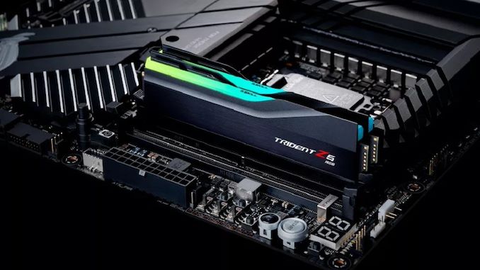
G.Skill Blitzes DDR5 World Record With Trident Z5 at DDR5-8888

https://ift.tt/3fX2Z9V

For users buying a memory kit of DDR5, if they want to adhere to Intel specifications, will buy a DDR5-4800 kit. Though through XMP, there are other faster kits available - we've even tested G.Skill's DDR5-6000 kit in our memory scaling article. But going above and beyond that, there's overclocking.

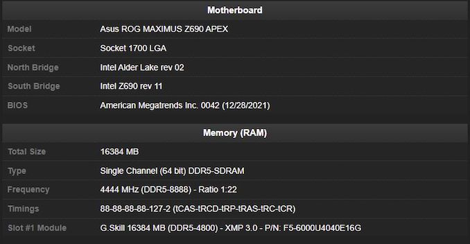
Back in November 2021, extreme overclocker 'Hocayu' managed to achieve DDR5-8704 using G.Skill's Trident Z5 DDR5-6000 memory. As always with these records, they are made to be broken, and fellow Hong-Kong native lupin_no_musume has managed to surpass this with an impressive DDR5-8888, also using G.Skill Trident Z5 memory, with an ASUS's ROG Maximus Z690 Apex motherboard, Intel's Core i9-12900K processor, and some liquid nitrogen.

Without trying to sound controversial, indeed, extreme overclocking isn't as popular as it once was. That isn't to say it doesn't have a purpose - using sub-ambient cooling methods such as liquid nitrogen, dry ice, and even liquid helium can boost frequencies on processors and graphics cards well beyond what's achievable with standard cooling. Doing this not only shows the potential of hardware, but it also gives companies 'bragging rights' as being the proud owners of overclocking world records. Car companies boast about the best Nürburgring record for a variety of categories, or tuning their mainstream offerings, in a similar fashion.


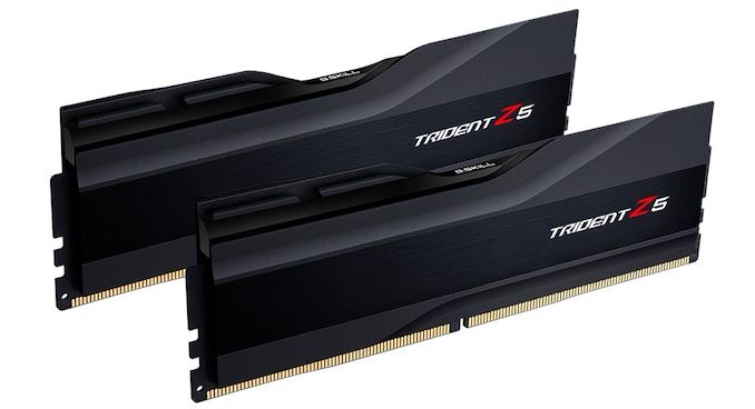
G.Skill Trident Z5 DDR5-6000 (2 x 16 GB) memory kit. 

This not only pushes the boundaries of what DDR5 memory is capable of, but it's also an impressive feat given DDR5 is relatively nascent. For reference, going from DDR5-6000 to DDR5-8888 represents an overclock of around 48% over the XMP profile and a crazy 85% overclock over the JEDEC specification of DDR5-4800. It should be worth noting that this is an all out data rate record regardless of latency, which in this case was increased to 88 over the standard 40, for stability. Going back to the car analogy, this would be akin to speed records on the drag strip, rather than on the oval.


Screenshot from G.Skill Trident Z5 DDR5-8888 CPU-Z validation (link)

While speeds of DDR5-8888 are not attainable in the form of purchasable memory kits for Alder Lake, G.Skill did unveil a retail kit that tops out at DDR5-7000. We also reported back in November 2021 that S.K. Hynix was planning for DDR5-8400 at 1.1 volts, but that's actually part of the entended JEDEC specifications for when processors get verfied at that speed.

Source: G.Skill

Related Reading


from AnandTech https://ift.tt/3nXeAdD
via IFTTT

Intel Alder Lake-H Core i9-12900HK Review: MSI's Raider GE76 Goes Hybrid

https://ift.tt/3447rRt

At CES this year, Intel officially announced its expanded Alder Lake lineup including the performance-laptop focused H-Series processors, which traditionally fit in the 45-Watt range. Today we finally get to take a look at the 12th generation H-Series processors, the first mobile incarnation of Alder Lake, and see how Intel's fastest mobile platform stacks up to not only Intel’s previous 11th generation Tiger Lake platform, but also AMD’s Ryzen 5000 series.


from AnandTech https://ift.tt/35nIRf6
via IFTTT

Monday 24 January 2022

NVIDIA’s GeForce RTX 3080 Ti is the fastest laptop for gamers and creators

https://ift.tt/3Aqj1Tf

NVIDIA’s latest GeForce RTX 30 Series laptop GPUs, first announced at this year’s CES, certainly sound impressive on paper. They’re built with Ampere - NVIDIA’s second-gen RTX architecture - which promises beautiful ray-traced graphics and cutting-edge AI features like DLSS, and they ship with 4th Generation Max-Q technologies that further enhance efficiency, performance, and battery life.

We’ve taken an early first look at the performance stats of the GeForce RTX 3080 Ti Laptop GPU and the new Max-Q technologies and are pleased to report some very impressive results.

NVIDIA GeForce RTX 3080 Ti: Gaming performance

The hike in performance delivered by the RTX 3080 Ti is no more evident than it is while gaming, with the laptop GPU delivering hugely impressive gains over the previous RTX 2080 SUPER GPU. In Assassin’s Creed: Valhalla, there is a whopping 1.53x improvement in gaming performance at ultra-high settings, while in DOOM Eternal there is an even more impressive 1.92x boost in performance from NVIDIA’s latest flagship laptop GPU. 

The RTX 3080 Ti handles everything thrown at it with ease; there’s a 1.56x performance increase in Call of Duty: Vanguard, a 1.66x increase in Cyberpunk 2077, and a jaw-dropping 2.3x increase in Metro Exodus Enhanced Edition when compared to the RTX 2080 SUPER-powered Razer Blade laptop. 

This massive performance boost isn’t all that is impressive about the RTX 3080 Ti. NVIDIA continues to lead the ray tracing race thanks to its 2nd-gen RT cores. NVIDIA’s DLSS makes games even faster; the AI rendering technology boosts frame rates using the RTX 3080 Ti’s dedicated Tensor Cores, so there’s no stress if you’re maxing out game settings.

NVIDIA GeForce RTX 3080 Ti: Creative apps 

NVIDIA GeForce RTX 3080 Ti powered laptops

(Image credit: NVIDIA)

The number of creators keeps growing rapidly. The RTX 3080 Ti is the best GPU for content creators, with dedicated hardware that accelerates video, ray tracing, and AI workflows, and with a huge 16GB of GDDR6 memory - the fastest memory ever shipped in a laptop. 

In Blender, the world's most popular 3D editing application, the RTX 3080 Ti-powered machine is 7.5X faster than the most expensive Apple MacBook Pro 16 with M1 Max. To put this in perspective, a 4 hour render on the MacBook Pro would be done in 30 minutes on the RTX 3080 Ti. On average, the RTX 3080 Ti is 7X faster than the MacBook Pro in 3D workloads.

These amazing speedups are thanks to improvements on NVIDIA’s Ampere architecture. Compared to the last generation, the RTX 3080 Ti outperformed the RTX 2080 SUPER by as much as 128% in Redshift Render, besting the MacBook by some 102%. Similarly, in Octanebench, the RTX 3080 Ti recorded performance gains of 100% compared to its predecessor. 

The RTX 3080 Ti also gives creators access to all of the NVIDIA Studio benefits, including accelerations on the top creative apps, ultra-reliable NVIDIA Studio drivers, and unique apps like NVIDIA Omniverse for 3D editors, NVIDIA Broadcast for live streamers and video editors, and NVIDIA Canvas for graphic designers. And it can be found in beautiful, purposely-made creator designs with incredible displays.

4th Generation Max-Q Technologies 

The RTX 3080 Ti is bolstered even further by NVIDIA’s new 4th generation Max-Q technologies, which utilise AI to deliver extreme efficiency in thin, high performance laptops. CPU Optimiser enables the GPU to optimise the performance, temperature, and power of the CPU to ensure your laptop’s CPU works more efficiently when gaming or creating. As power is saved, it is shifted between the CPU and GPU to improve performance. Rapid Core Scaling offers significant benefits for creators; it scales the optimal number of cores and operates them at higher frequencies, delivering more performance for intensive creative work and STEM apps while on battery power. 

NVIDIA GeForce RTX 3080 Ti powered laptops

(Image credit: NVIDIA)

Max-Q technologies are also lifesavers when you’re running on the laptop's battery. Max-Q’s improved Battery Boost 2.0 finds the optimal balance of GPU and CPU power usage, battery discharge, image quality, and frame rates for longer battery life. NVIDIA claims that with this feature enabled you’ll get up to 70% more gameplay from your laptop whilst on battery.

The GeForce RTX 3080 Ti is a force to be reckoned with, judging by these specs, and whether its for gaming, creativity or STEM work, it seems like you’ll struggle to find a performance to match. Stay tuned for new laptop system reviews featuring the NVIDIA GeForce RTX 3080 Ti and other GeForce RTX GPUs starting tomorrow.


from TechRadar: computing components news https://ift.tt/3FWU6Yn
via IFTTT

Interview with Intel’s Dan Ragland, Head of Overclocking: Tuning Alder Lake For Performance

https://ift.tt/3nSPe06

The topic of overclocking has been an interesting one to track over the years. Over a decade ago, when dealing with 2-4 core processors, an effective overclock gave a substantial performance uplift, often allowing a $200 processor to perform like the one that cost $999. However, core counts have increased over the last couple of years, but also companies like Intel are getting better at understanding their silicon, and are able to ship it out of the box almost at the silicon limit anyway. So what use is overclocking? We turned to Dan Ragland, who runs Intel’s Overclocking Lab in Hillsboro, Oregon, to find out what overclocking now means for Intel, what it means for Alder Lake, but also how Intel is going to approach overclocking in the future.


from AnandTech https://ift.tt/3rO3cS6
via IFTTT

Sunday 23 January 2022

Intel Alder Lake Core i5 CPU you can’t buy hits a staggering 5.7GHz overclock

https://ift.tt/eA8V8J

An Intel Alder Lake Core i5 processor which is a non-K model – meaning it isn’t unlocked, so shouldn’t be able to be overclocked – has been clocked up to new heights, but note that this CPU is only available to buy in Asia.

There are a couple of things to unpack here, and firstly that’s the exact model in question which is the Core i5-12490F, a chip with six-cores (all performance, with no efficiency cores) that’s only on sale in China. Further remember that processors which aren’t unlocked ‘K’ models (this one is ‘F’, meaning it has no integrated graphics) shouldn’t be able to undergo overclocking as mentioned, but they can thanks to an unofficial way of using the Unlock BCLK feature in the BIOS on some motherboards (Z690 or B660 chipsets).

So, what’s happened here is that some enterprising owner has taken Der8auer’s BCLK method and juiced this Core i5 Alder Lake CPU up to 5.7GHz, which is way above its default clock speed of 3GHz (nearly double, in fact), and a huge chunk more than the maximum boost of 4.6GHz.

As Tom’s Hardware, which spotted that leaker Tum_Apisak had highlighted this overclocking feat on Twitter, points out, the BCLK was set to 142.53MHz and voltage ramped up to a massive 1.696V. This means some kind of exotic cooling must have been used, as any standard methods wouldn’t give the headroom to push nearly this hard – although sadly no details of the actual cooling employed were provided.


Analysis: Major overclocking potential, but with an equally major caveat

Once again, another big overclock – joining the Core i3-12300 which was clocked up to be the world’s speediest quad-core CPU earlier this week – shows the potential of these 12th-gen non-K processors to be serious performers. As we mentioned above, the cooling used here isn’t made clear, but in that Core i3 effort, dry ice was used to provide super-cool conditions.

Even with normal cooling, non-K Alder Lake chips have a good deal of potential to be ramped up, in theory – but there’s one fly in the ointment. Namely that Intel just came out and said that such non-K CPUs are not designed to be overclocked, and that powering them up in this way could “damage or reduce the useful life of the processor and other system components, and may reduce system stability and performance.”

In other words, you have been warned about the dangers here, and the processor’s warranty will be voided too. It seems likely that Intel will patch out the ability to perform these BCLK overclocks on non-K CPUs before long via BIOS updates in the future, so we wouldn’t bank on this workaround being present for all that long.


from TechRadar: computing components news https://ift.tt/3rGNV5Q
via IFTTT

Friday 21 January 2022

Intel Announces Ohio Fab Complex: 2 New Fabs For $20B, And Space For More

https://ift.tt/2WnDubk

With fab expansions on tap across the entire semiconductor industry, Intel today is laying out their own plans for significantly increasing their production capacity by announcing their intention to build a new $20 billion fab complex in Ohio. With the paperwork already inked and construction set to begin in late 2022, Intel will be building two new leading-edge fabs in their new Ohio location to support future chip needs. And should further demand call for it, the Ohio complex has space to house several more fabs.

Intel’s announcement follows ongoing concerns about chip fab capacity and national security, as like other chip fabs, Intel is looking to expand their capacity in future years amidst the current chip crunch. All the while, the United States government has become increasingly mindful about how much chip production takes place in geopolitically tricky Taiwan, placing additional pressure on firms to build additional fabs within the US. To that end, Intel has been not-so-secretly undertaking a search to find a good location for a new fab campus, and they have finally found their answer in Ohio.

The new site, Intel’s first new manufacturing site location in 40 years, is located in New Albany, Ohio, just outside of Columbus. Up until now, all of Intel’s major chip fab sites have been in the western United States – Oregon, Arizona, and at one point, Silicon Valley – so the Ohio site is a significant move for the company. All told, the Ohio “mega-site”, as Intel likes to call it, covers nearly 1000 acres. And while Intel is only initially planning for two fabs, the site offers plenty of room to grow, offering enough space for a total of 8 fabs.

The immediate goal of the company – and the crux of today’s announcement – revolves around the building of two new leading-edge fabs at the Ohio location. According to Intel, these two fabs will begin construction late this year, with production coming online in 2025. The company isn’t formally stating what the initial process node will be – instead saying that it will be using the "industry's most advanced transistor technologies" – however if the company is indeed building truly bleeding-edge fabs, then 2025 lines up with Intel’s 18A process, which will be 4 generations newer than what Intel is using now (Intel 7).
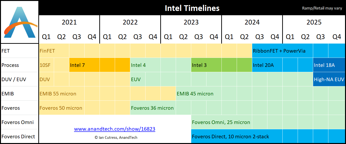
Altogether, Intel expects the project to cost about $20 billion, which is similar to what Intel will be spending for its two new Arizona fabs, which were announced just under a year ago. And further down the line, should Intel opt to fill the rest of the property with the other 6 fabs that the site can support, the company expects that the total price tag could reach nearly $100 billion. Ultimately, the company is making it clear that they are priming the site not just to met their mid-term production needs with the initial two fabs, but are making sure to have the space ready for further capacity expansion over the long-term.

As to whether Intel eventually builds those further 6 fabs, that will depend on a few factors. Key among these will be demand from Intel Foundry Services clients; while Intel will be using some of the Ohio site’s capacity for their own needs, the site will also be used to fab chips for IFS customers. If Intel’s bid to break into the contract fab business is successful, and the company is able to woo over additional clients/orders, then they will need to build additional fabs to meet that demand.

Also hanging in the balance is what the US Government opts for, both in terms of orders and incentives. The Ohio fabs will be used for domestic production of sensitive chips, as the US looks to secure its supply lines. Meanwhile the CHIPS for America Act and its 53 billion in incentives will also be a. Intel for its part isn’t playing coy about its interest in the CHIPS money, explicitly stating that “The scope and pace of Intel’s expansion in Ohio, however, will depend heavily on funding from the CHIPS Act”. In some respects Intel is taking a bit of a gamble by investing in the Ohio location before any CHIPS funding is approved – on a pure cost basis, overseas production is traditionally cheaper – so there is certainly a political element in announcing these fabs and selecting an Ohio location. And as an added incentive to the US Government, Pat Gelsinger has told Time that Intel would even be interested in bringing some chip packaging, assembly, and testing back to the US if the CHIPS Act were funded, which in turn would allow Intel to do every last step of production within the US.

But more immediately, Intel’s focus is on getting its first two Ohio fabs up and running. Along with building the facilities they’ll need a workforce to operate them, and as a result the company is also pledging $100M over a decade in funding for local educational efforts. As with similar local industry efforts, that investment would be focused on helping local colleges and universities establish semiconductor manufacturing curricula to help train the technical workforce required.

And while outside of Intel’s own investment scope, the creation of their Ohio fab complex means that Intel’s suppliers are also coming along for the ride. According to the company, Air Products, Applied Materials, LAM Research and Ultra Clean Technology have all indicated that they’ll be setting up facilities in the area. All of which the company is using to further underscore the size of the project and the value it brings to the area – and why they deserve that CHIPS Act funding.

Ultimately, the addition of a third US fab site and two more fabs to Intel’s portfolio is the latest step Intel has taken under Pat Gelsinger’s IDM 2.0 strategy. Gelsinger opted to go all-in on having Intel fab chips for themselves and others, and this is the kind of expansion that Gelsinger has been alluding to as necessary to make IDM 2.0 a reality. Taken altogether, Intel now has 4 leading-edge fabs set to come online in the 2024-2025 timeframe, and with any luck on Intel’s part, there will be room for several more to come.

Source: Intel


from AnandTech https://ift.tt/3AkiwKh
via IFTTT
Intel Alder Lake CPU overclocking trick works with cheaper motherboards (but there’s a catch)

https://ift.tt/eA8V8J

Intel’s Alder Lake non-K processors can be overclocked as we’ve seen in recent times – when it should only be unlocked ‘K’ models that can do this, traditionally – and it has now emerged that this trick works with mid-range motherboards too.

Der8auer is the expert overclocker who has been working away at juicing up Alder Lake CPUs like the Core i5-12400, and even a lowly Celeron model, but previously it was thought that these chips could only be overclocked in a high-end Z690 motherboard with support for BCLK unlock.

You may recall that Der8auer theorized that B660 motherboards should allow for non-K processors to be overclocked like this, and indeed the German overclocker has now proved this, achieving the feat with two different Asus ROG Strix B660 motherboards as VideoCardz spotted.

So, buying one of these cheaper mid-range B660 models – rather than forking out megabucks for a Z690 – and pairing it with an affordable Core i5 (or Core i3) non-K Alder Lake CPU with a big overclock is indeed possible - all for a relatively modest outlay.

Well, sort of, because as we noted in the headline above, there’s a catch, and a fairly substantial one: Der8auer says he hasn’t found a DDR4 supporting B660 board that offers this overclocking ability, only DDR5-ready models.


Analysis: DDR5 costs are prohibitive – but don’t lose all hope

As this is apparently DDR5-only, that presents a big problem in that this system RAM is not easy to find, and very expensive, as it’s still early days for the new memory sticks. As ever, when a new RAM standard emerges, you can expect to pay well over the odds to get hold of the memory modules.

So, regarding the idea of a Core i5 Alder Lake system for a modest outlay, going the B660 route, that’s rather scuppered by the price you’ll have to pay for the DDR5 memory that will be the only choice to fit the motherboard.

All hope of pulling off a more wallet-friendly overclockable non-K rig isn’t lost, though, because it may yet turn out that there is a DDR4 supporting board which also has the capability for a BCLK unlock in the BIOS. And even if there isn’t – let’s face it, Der8auer does not seem optimistic about that – then we must bear in mind that DDR5 availability and pricing will get better as time goes on (and also when component shortages become less of a concern, which could hopefully happen later in 2022).

If all that pans out, then we could still be looking at some interesting possibilities for big overclocks in modest systems, maybe with Raptor Lake CPUs. Intel’s next-gen chips are expected to arrive later in 2022, of course, being pretty much a refresh of Alder Lake (but speedier, naturally), and therefore it could be expected that they will keep this unlocking functionality. That said, there’s no guarantee Intel will keep these overclocking possibilities in for Raptor Lake.

We’ll just have to see, but meantime, it’s still fascinating to witness the kind of overclocking which can be achieved with non-K Alder Lake silicon, which has already led to a world record overclock with the Core i3-12300 (absolutely destroying the previous quad-core record holder, the AMD Ryzen 5300G).


from TechRadar: computing components news https://ift.tt/3IukjiT
via IFTTT

Wednesday 19 January 2022

Intel Expands 12th Gen Core to Ultraportable Laptops, from 5-cores at 9 W to 14-cores at 28 W

https://ift.tt/3tEk942

Over the years Intel has prided itself on its ability to provide processors that fit into the ultraportable, professional market. We’re talking thin and light designs with obscene levels of performance and battery life for the form factor. It’s so important to Intel, that over the years they’ve produced several design and validation standards relating to how the best ultraportables should be developed, such as low power displays, the best connectivity standards, and approaching all-day battery life. It surprised me somewhat that Intel didn’t really discuss its next generation of processors for these devices at CES at the beginning of the year, focusing their keynote almost entirely on the 45 W prosumer and workhorse designs instead. To find out about the more mainstream and ultraportable silicon, we had to dig into the back end of our press deck to get details.


from AnandTech https://ift.tt/3GYiri5
via IFTTT

Tuesday 18 January 2022

Intel’s lowly Celeron G6900 CPU gets overclocked to a staggering 5.3GHz

https://ift.tt/eA8V8J

Intel’s lowly Celeron G6900 processor can be pepped up massively, an expert overclocker has shown us, pushing the Alder Lake chip to a rather staggering 57% above its default clock speed.

This feat was achieved by Der8auer, a well-known German overclocker who has set many previous records when juicing up chips, and managed to get the G6900 CPU to hit 5,338MHz (up from the default base clock speed of 3.4GHz).

What’s even more interesting here, aside from a low-end chip blazing away at over 5.3GHz, is that of course this is a non-K processor – only Intel’s ‘K’ model CPUs are officially able to be overclocked. However, with Alder Lake, other models can be ramped up, at least if they’re running on a Z690 (high-end) motherboard, using the BCLK unlock capability in the BIOS (BCLK meaning base clock).

Recently Der8auer has also demonstrated overclocking other Alder Lake non-K processors including Intel’s Core i5-12400, with seriously impressive results (reaching 5,240MHz across all cores). Plus in this new video, he shows the Intel Core i3-12100 hitting 5,400MHz – about 26% faster than its rated boost.


Analysis: This trick might apply outside top-end motherboards, too

Taking that last point, it’s worth noting that the Core i3-12100 running at 5.4GHz with all-cores managed to pretty much keep pace with the AMD Ryzen 5 5600X in Cinebench R20 multi-thread. Given the big price difference here – the Ryzen processor costs around twice as much – that’s seriously impressive, although remember overclocking results with the 12100 will vary (depending on the quality of the chip), and this is just a single benchmark (gaming performance for example will doubtless be very different).

Still, even given those caveats, the overclocking of Alder Lake chips via BCLK would appear to provide a sizeable dollop of extra performance mileage for those with a good enough motherboard. And it’s certainly eye-opening to see a Celeron hit such speeds – not that the G6900, as a dual-core CPU, is any great shakes for, say, the likes of gaming even at high clock speeds (and of course you’d never pair such a chip with the necessary high-end motherboard in the real world).

Speaking of motherboards, Der8auer used a couple of Asus Z690 models when testing these overclocks so far, but theoretically other boards – and those from different manufacturers – should work too, or at least some of them (note that the overclocking expert failed to achieve the feat on a couple of other Asus mobos). Apparently, it could be the case that the necessary capability in determining whether non-K overclocking is possible may be an external clock generator, as this might be required for the Unlock BCLK feature in the BIOS.

Although as Tom’s Hardware, which spotted this, points out, in theory Intel has previously said that such an external clock generator wouldn’t be necessary for overclocking, and that a ‘synthetic BCLK’ could allow for tweaking on motherboards that don’t have one.

At any rate, there’s also the exciting possibility that this kind of overclock could be possible on lower-end boards with Alder Lake. Indeed, in Der8auer’s YouTube video comments, he notes that he’s found two B660 motherboards that “should technically” allow for non-K overclocking like this. These have been ordered, and Der8auer is hoping to provide an update on whether he can pull this off in the next few days.


from TechRadar: computing components news https://ift.tt/3IgWX04
via IFTTT

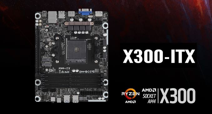
ASRock Unveils DeskMeet SFF PC Platform with Intel B660 / AMD X300 Chipsets

https://ift.tt/3rn6ADs

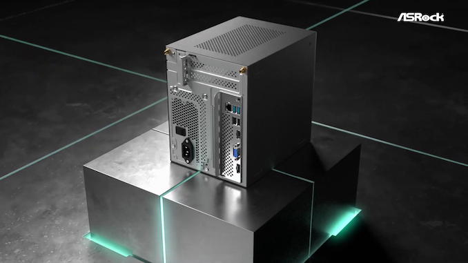
ASRock has been at the forefront of the small form-factor (SFF) PC revolution right from the Sandy Bridge days. Starting with the Core HT series in the early 2010s, the company moved on to the Beebox (NUC clones) , and recently settled on the DeskMini lineup (based on mini-STX boards). At the 2022 CES, the company is introducing a new SFF PC - the DeskMeet. It is meant to be a step up from the DeskMini - allowing for a custom motherboard, more RAM slots, and space for discrete GPUs.

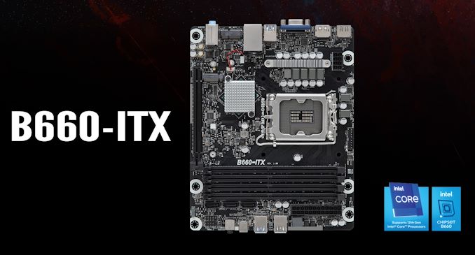
ASRock is delivering all this in a chassis with a 8L volume with two configurations - one based on the Intel B660 platform, and another based on the AMD X300 chipset (AM4 socket). The key specifications of the two systems are summarized in the table below.

ASRock DeskMeet SFF PCs - 2022 Lineup
  DeskMeet B660 DeskMeet X300
CPU Intel 12th Gen Core Processors AMD AM4 Socket Ryzen Desktop APUs / CPUs (Ryzen 2000/3000/4000/5000) (up to 65W)
Cooler Stock coolers / up to 54mm in height
Chipset Intel B660 AMD X300
Memory Dual-Channel DDR4
4x DDR4 DIMM Slots (up to 128GB)
non-ECC, un-buffered
Dual-Channel DDR4
4x DDR4 DIMM Slots (up to 128GB)
ECC / non-ECC, un-buffered
Discrete GPU Support Up to 200mm in length
Networking 1x RJ-45 Gigabit LAN (Intel I219V)
M.2 2230 Slot for Wi-Fi + BT Module
1x RJ-45 Gigabit LAN (Realtek RTL8111H)
M.2 2230 Slot for Wi-Fi + BT Module
Storage 3x SATA III 6Gbps
1x Hyper M.2 2280 (PCIe Gen 4 x4 / SATA III 6Gbps)
1x Hyper M.2 2280 (PCIe Gen 4 x4)
2x SATA III 6Gbps
1x Ultra M.2 2280 (PCIe Gen 3 x4)
Expansion Slots 1x PCIe 4.0 x16 1x PCIe 3.0 x16
Audio Codec Realtek ALC897
Front I/O 1x Headset
1x USB 3.2 Gen 1 Type-C
2x USB 3.2 Gen 1 Type-A
2x USB 2.0 Type-A
Rear I/O 1x DP 1.4a
1x HDMI 2.0a
1x D-Sub
2x USB 2.0 Type-A
2x USB 3.2 Gen 1 Type-A
1x RJ-45<
HD Audio Jack (Line In / Speaker / Microphone)/td>
1x DP 1.4a
1x HDMI 2.0a
1x D-Sub
2x USB 2.0 Type-A
2x USB 3.2 Gen 1 Type-A
1x RJ-45<
HD Audio Jack (Line Out)/td>
Power Supply 500W (80+ Bronze / 550W Peak)
Dimensions 168mm x 219.3mm x 218.3mm

While the absence of high-end I/O ports like Thunderbolt 4 and USB 3.2 Gen 2x2 or high-end wired networking is a tad disappointing, ASRock is making up for that by supporting PCIe expansion cards and quad-DIMM configurations for up to 128GB of RAM. ASRock calls these boards -ITX, but they are not truly mini-ITX in size.

The space inside the chassis allows for multiple configurations - with or without a discrete GPU, ability to mount multiple 3.5" drives etc. The DeskMeet aims to provide as many features and flexibilities as possible within the constraints dictated by the chipsets.

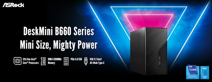
In other ASRock SFF PC news, the company has also released a new mini-STX platform using the Intel B660 chipset for Alder Lake. The DeskMini B660 retains the chassis design of the previous generations.

Thanks to the use of the B660 chipset, the front Type-C port is now USB 3.2 Gen 2x2 (20 Gbps). The rear Type-C port supports 10 Gbps data transfer alone with DP 1.4a, and 60W PD. The other interesting aspect is the availability of a PCIe 5.0 M.2 2280 SSD slot, in addition to a PCIe 4.0 M.2 2280 one. A M.2 2230 slot for Wi-Fi, and a gigabit Ethernet slot are the regular features retained from the previous DeskMini units.

After a couple of years of staid SFF PCs with rather unimpressive updates, ASRock is promising interesting offerings in 2022. No specific launch prices or retail availability timelines were provided for the new systems.


from AnandTech https://ift.tt/3qAFY2I
via IFTTT

Sunday 16 January 2022

Nvidia RTX 3090 Ti leaked pricing suggests a wallet-damaging GPU

https://ift.tt/eA8V8J

Nvidia RTX 3090 Ti pricing has leaked from some European retailers, and it seems the new flagship graphics card could perhaps take a chunkier bite out of your wallet than you might expect compared to the vanilla RTX 3090 (although then again, you may well have prepared yourself for the worst anyway, if you were mulling buying this new top-end Ampere offering).

As VideoCardz reports, purported prices have been spilled from at least two Swiss retailers and a German outlet (or at least the site is in German), and converted pricing (from Swiss Francs or Euros) gives a range of price tags from about $3,500 (around £2,560, or AU$4,860) to $4,500 (around £3,290, or AU$6,240).

Admittedly, two of the four prices mentioned – all of which are for MSI’s GeForce RTX 3090 Ti Suprim X, except in one case, where it’s MSI’s Gaming X Trio model – are at the lower end of the scale, but clearly these are going to be costly cards if these retailers are correct.

Naturally, we must be very cautious around any pre-release pricing, because often these tags can be mere placeholders, or to put it another way, guesswork, really. Certainly in the past such leaked figures have turned out to be wrong, but that said, even if errant, they can still be a useful ballpark figure.

Rather than try to rely on generally shaky currency conversions, VideoCardz also observes that in the case of the German site, an RTX 3090 (from Zotac) is listed for comparative pricing, and the 3090 Ti from MSI (Gaming X Trio) is 31% more expensive. That could be a more telling comparison, but again, exercise a great deal of caution around all of this.


Analysis: The specter of thin supply and price inflation looms again

We didn’t really expect anything but a weighty asking price for the RTX 3090 Ti, of course, and it’s a fair guess that supply-wise, retailers likely aren’t going to be getting a large number of them – what with Nvidia’s ongoing inventory and production woes that aren’t expected to resolve until the second half of this year – so retailers will be looking to maximize profits on the stock they do receive. (Also, remember the most recent 3090 Ti news we heard, about purported production snags which may delay the arrival of the Ampere GPU – it’s expected, or was expected, to pitch up at the end of January).

If a price jump in the order of 30% does come to pass for the 3090 Ti – bearing in mind the caveats we’ve already underlined above – the performance increase the card provides at these dizziest heights of GPU pricing isn’t likely to add up. Particularly when as one VideoCardz reader points out in the comments, for around the same money (in US dollars) you can buy an Alienware gaming PC with not just an RTX 3090, but a Core-i9 11900KF CPU and all the other trimmings (including 32GB of system RAM).

Such is the world of graphics card pricing we live in today, but that said, there will still be PC enthusiasts out there willing to pay whatever it takes to get the top dog Ampere card, no doubt.


from TechRadar: computing components news https://ift.tt/3KiWqw6
via IFTTT

Saturday 15 January 2022

Intel Raptor Lake CPUs could be good news for gamers

https://ift.tt/eA8V8J

Intel’s next-gen Raptor Lake processors could boost on-board cache considerably compared to Alder Lake, if a new rumor is right.

This one was tweeted by hardware leaker OneRaichu, with the claim that Raptor Lake desktop will ramp up cache to 68MB.

See more

As explained in the Twitter thread, this doesn’t include L1 cache, meaning it’s L2 and L3 (the latter are larger amounts of memory, but slower – L1 is the fastest CPU cache, but smallest).

Raptor’s purported 68MB configuration compares to 44MB for Alder Lake (which is divided into 30MB of L3, and 14MB of L2), so this would be an over 50% increase for the next-gen chips, an impressive leap.


Analysis: Cranking up the cache with Raptor – and more besides?

This isn’t the first time we’ve heard about Intel planning to seriously boost levels of CPU cache with Raptor Lake. Back in March 2021, almost a year ago now, a leak put forward the assertion that we’d see an “improved CPU cache for gaming” with 13th-gen silicon.

The additional cache – if this is true, and despite having heard a couple of rumors now, we must still remain skeptical – will be a good way to improve Raptor Lake for gamers, as well as the IPC (instructions per clock) gains that a new generation of silicon will inevitably achieve. Remember, Raptor Lake will just be a refresh of Alder Lake architecture, so these areas are where all the performance gains will come from.

That, and upping the ante when it comes to core configurations and clock speeds, of course (though likely the latter will only be a very modest boost). Elsewhere the CPU grapevine has floated the idea that the 13th-gen flagship will be a 24-core CPU, with 8 performance cores and 16 efficiency cores, so in the latter case, that would be double what the current 12900K has – a hefty boost.

Raptor Lake chips are due to arrive later this year, possibly in Q3 2022.

Via Wccftech


from TechRadar: computing components news https://ift.tt/3fo5bah
via IFTTT

Friday 14 January 2022

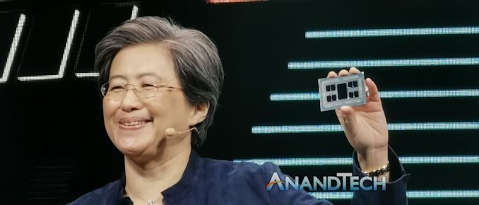
How Low Cost Can Chiplets Go? Depends on the Optimization, says AMD’s CEO Dr. Lisa Su

https://ift.tt/3fvvf2Z

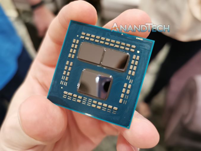
While not the absolute first company in the market to talk about putting different types of silicon inside the same package, AMD’s launch of Ryzen 3000 back in July 2019 was a first in bringing high performance x86 computing through the medium of chiplets. The chiplet paradigm has worked out very well for the company, having high performance cores on optimized TSMC 7nm silicon, while farming the more analog operations to cheaper GlobalFoundries 14nm silicon, and building a high speed interconnect between them. Compared to a monolithic design, AMD ends up using the better process for each feature, smaller chips that afford better yields and binning, and the major cost adder becomes the packaging. But how low cost can these chiplet designs go? I put this question to AMD’s CEO Dr. Lisa Su.

In AMD’s consumer-focused product stack, the only products it ships with chiplets are the high-performance Ryzen 3000 and Ryzen 5000 series processors. These range in price from $199 for the six-core Ryzen 5 3600, up to $799 for the 16-core Ryzen 9 5950X.

Everything else consumer focused is a single piece of silicon, not chiplets. Everything in AMD’s mobile portfolio relies on single pieces of silicon, and they are also migrated into desktop form factors in AMD’s desktop APU strategy. We’re seeing a clear delineation between where chiplets make financial sense, and where they do not. From AMD’s latest generation of processors, the Ryzen 5 5600X is still a $299 cost at retailers.

One of the issues here is that a chiplet design requires additional packaging steps. The silicon from which these processors are made have to sit in a PCB or substrate, and depending on what you want to do with the substrate can influence its cost. Chiplet designs require high speed connections between chiplets, as well as power and communications to the rest of the system. The act of putting the chiplets on a singular substrate also has an effective cost, requiring accuracy - even if 99% accurate placement per chiplet on a substrate means a 3 chiplet product as a 3% yield loss from packaging, raising costs. Beyond this, AMD has to ship its 14nm dies for its products from New York to Asia first, to package them with the TSMC compute dies, before shipping the final product around the world. That might be reduced in future, as AMD is set to make its next-generation chiplet designs all within Asia.

Ultimately there has to be a tipping point where simply building a monolithic silicon product becomes better for total cost than trying to ship chiplets around and spend lots of money on new packaging techniques. I asked the question to Dr. Lisa Su, acknowledging that AMD doesn’t sell its latest generation below $300, as to whether $300 is the realistic tipping point from the chiplet to the non-chiplet market.

Dr. Su explained how in their product design stages, AMD’s architects look at every possible way of putting chips together. She explained that this means monolithic, chiplet, packaging, process technologies, as the number of potential variables in all of this have direct knock-on effects for supply chain and cost and availability, as well as the end performance of the product. Dr. Su stated quote succinctly that AMD looks for what is best for performance, power, cost – and what you say on the tipping point may be true. That being said, Dr. Su was keen not to directly say this is the norm, detailing that she would expect in the future that the dynamic might change as silicon costs rise, as this changes that optimization point. But it was clear in our discussions that AMD is always looking at the variables, with Dr. Su ending on a happy note that at the right time, you’ll see chiplets at the lower end of the market.

Personally, I think it’s quite telling that the market is very malleable to chiplets right now in the $300+ ecosystem. TSMC D0 yields of N7 (and N5) are reportedly some of the industry best, which means that AMD’s mobile processors in the ~200 sq mm range can roll off the production line and cater for everything up to that $300 value (and perhaps some beyond). Going bigger brings in die size yield constraints, where chiplets make sense. We’re now in at a stage where if Moore’s Law continues, how much compute can we fit in that 200 sq mm sized silicon, and which markets can benefit from it – or are we going to get to a point where so many more features are added that silicon sizes would increase, necessarily pushing everything down the chiplet route. As part of the discussion, Dr. Su mentioned economies of scale when it comes to packaging, so it will be interesting to see how this dynamic shakes out. But for now it seems, AMD’s way to address the sub-$300 market is going to be with either last generation hardware, or monolithic silicon.


from AnandTech https://ift.tt/3GAXWYA
via IFTTT

Tuesday 11 January 2022

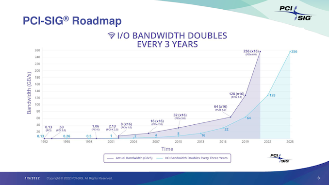
PCIe 6.0 Specification Finalized: x16 Slots to Reach 128GBps

https://ift.tt/3r5PFoJ

This morning the PCI Special Interest Group (PCI-SIG) is releasing the much-awaited final (1.0) specification for PCI Express 6.0. The next generation of the ubiquitous bus is once again doubling the data rate of a PCIe lane, bringing it to 8GB/second in each direction – and far, far higher for multi-lane configurations. With the final version of the specification now sorted and approved, the group expects the first commercial hardware to hit the market in 12-18 months, which in practice means it should start showing up in servers in 2023.


from AnandTech https://ift.tt/3Fh73vO
via IFTTT

AMD Ryzen 7 5800X3D CPU could be in short supply when it launches

https://ift.tt/eA8V8J

AMD’s Ryzen 7 5800X3D, the new 3D V-cache processor revealed at CES, may only be produced in small numbers when it lands in early 2022 – and the chip may remain thin on the ground until the second half of the year rolls around, going by the latest from the rumor mill.

This comes from DigiTimes (via PC Gamer), which reports that TSMC, which is making the 5800X3D, is only expected to kick off with ‘small-volume production’ of the processor, according to the usual industry sources in the know. However, the report also makes clear that production could ramp up considerably when TSMC’s new packaging plant in Chunan (Taiwan) goes live later in the year (supposedly in the second half of 2022).

So, while everyone is (rightly) cautious about the potential amount of stock when it comes to many new PC components at launch, it appears that the Ryzen 7 5800X3D could be particularly shaky to begin with – perhaps for the first few months of the CPU being on shelves (or not, as the case may be).

At least if this report is correct, anyway; and note we certainly must be cautious on that score, as DigiTimes isn’t always the most reliable media outlet.


Analysis: Could 3D V-cache turn out to be a rather ineffective stopgap?

We – and a good number of other folks, no doubt – were a little taken aback when AMD’s CES 2022 3D V-cache refresh turned out only to involve revamping the one model. However, if there are rumblings from the supply chain rumor peddlers that AMD could struggle getting enough of just the 5800X3D out there, then it’s no real surprise that Team Red didn’t also see fit to push out a 5900X3D or a 5950X3D (or any other variant, for that matter).

We know that component shortages are making life difficult for AMD (and everyone else) anyway, certainly for the first half of this year, and as PC Gamer points out, the company has to prioritize enterprise chips (Epyc) to a large extent at the high-end as these are big profit spinners.

We mustn’t read too much into this as we’ve already mentioned, but if this does pan out to be the truth – or something close to it – it’ll leave this 3D V-cache overhaul looking like a rather ineffective stopgap measure against Intel’s impressive new Alder Lake chips. AMD’s Zen 4 processors are still a good way off, and not due until later in 2022, after all (and Intel’s next-gen Raptor Lake will arrive around the same time as them, or thereabouts, too, so Team Blue won’t be standing still).


from TechRadar: computing components news https://ift.tt/3tdJ66p
via IFTTT

Intel Alder Lake CPUs are now fixed for all games with DRM

https://ift.tt/eA8V8J

Intel has announced that any remaining DRM issues with Alder Lake processors are now resolved, so there are no longer any games that don’t work with the 12th-gen chips.

As you’re likely aware, there were reports of potential compatibility issues with DRM-toting games even before Alder Lake was released, and after the processors went on sale, we found out that 90+ games had DRM gremlins that either meant they kept crashing, or wouldn’t even load up full-stop.

However, as flagged up by @davideneco25320 on Twitter, Intel has now cured all these issues. To be fair to Team Blue, as of a month ago, the vast majority of games were fixed to work with 12th-gen CPUs; all but three of them, in fact, and those outliers have now been rectified. (They were Assassin’s Creed: Valhalla, Fernbus Simulator, and Madden 22, if you’re curious).

The chip giant updated its support document on the bugbear to say: “Intel has resolved the DRM issue on 12th Gen Intel Core Processors that caused games to crash or not load in Windows 11 and/or Windows 10 by working with game publishers and Microsoft. At this time, all games originally identified as having this DRM issue have been fixed through game patches or OS updates.

“If you experience issues on an older Windows OS, run the latest version of Windows Update to resolve the issue. Along with game patches, the most recent updates for Windows 11 and Windows 10 have resolved a majority of the DRM issues.”


Analysis: BIOS workaround is no longer needed, thankfully

The problems with these games were wrapped up in the DRM software not recognizing Alder Lake processors as one single CPU, but instead detecting the efficiency cores as another chip.

So, in other words, the DRM was finding two CPUs in operation, thinking something was, therefore, suspect with two separate chips apparently running the game, and throwing a wobbler, either refusing to load the title or crashing out.

This was why the previous workaround was simply to turn off those efficiency cores (in the BIOS by enabling ‘Legacy Game Compatibility Mode’), obviously at something of a performance hit.

The good news now for the many Assassin’s Creed: Valhalla fans out there is that they’ll no longer have to drop any fps with an Alder Lake CPU. According to reports, this has actually been the case for a couple of weeks or so now, so Intel was pretty quick to fix up this problem overall. That said, arguably it should’ve ideally been ironed out before release.

Via VideoCardz


from TechRadar: computing components news https://ift.tt/3f8ZE7n
via IFTTT

Monday 10 January 2022

Intel Changes Senior Executives: VP That Led CES is Out, New CFO

https://ift.tt/3zNc0vd

At the close of play today, Intel is announcing two major changes at the top of its organization. The big one is that EVP and GM of Intel’s Client Computing Group, Gregory Bryant, who led the company in their CES messaging only last week, is moving on to new ventures. After his 30-year stint at Intel, he is to be replaced by 25-year veteran Michelle Johnston Holthaus, currently EVP and Intel’s Chief Revenue Officer in charge of Communications, Sales, and Marketing. There’s also a new CFO coming in from Micron.

It’s a big surprise, seeing Gregory Bryant leave Intel. He has been leading the consumer platform team for a number of years, since June 2017, covering the last few generations of CPU and mobile launches through Intel’s tough times with bringing 10nm to revenue. He has overseen the launch of the Intel Evo initiative, and comes from an engineering background, although preferred to let other senior engineers talk to their strengths. Greg will leave Intel at the end of the month, for a new opportunity. It's actually quite a strange announcement, given that he led Intel's presentations at CES only last week - a time when he must've known that one foot was out the door. Analysts are reporting that his goals involve becoming a CEO somewhere, and that the opportunity he is leaving for is a big one. It also reduces the number of Bryants at senior levels of Intel down from three to one (Diane Bryant left in 2017).

Bryant’s replacement is Intel EVP and Chief Revenue Officer Michelle Johnston Holthaus. She is another Intel lifer, having spent 25 years at the company, joining in 1996. She has held multiple roles in reseller management, HQ central marketing and operations, global account management, and currently sits as GM of the Sales, Marketing, and Communications group. In recent memory Holthaus was the keynote speaker at Intel’s Partner Summit. Bringing her to the role is likely a move to strengthen Intel’s bonds with its OEM partners, an aspect that is seeing increased competition in traditional client OEM markets. It also means that Intel has two women leading its largest business units – Holthaus for Client Computing, and Sandra Rivera for Datacenter.

During the transition, Intel will be searching for a new leader of Intel’s sales, marketing, and communications group.

Also announced today is that Intel is to get a new Chief Financial Officer. It was already announced that current CFO, George Davis, was to retire in 2022 and the search was on for a replacement. That replacement has been found in the form of David Zinsner, who comes from his role as CFO at Micron. This position is effective January 17th, which is shortly before Intel’s end-of-year financial results on January 26th. George Davis is to remain at Intel in an advisory role until May to ensure a seamless transition. It’s key to point out that Intel’s search for a new CFO has been thought to aim to find an individual who has the same CAPEX expenditure aspirations as CEO Pat Gelsinger.


from AnandTech https://ift.tt/3GidW1a
via IFTTT

AMD: We’re Using an Optimized TSMC 5nm Process

https://ift.tt/3r7Nelw

When AMD started using TSMC’s 7nm process for the Zen 2 processor family that launched in November 2019, one of the overriding messages of that launch was that it was important to be on the leading edge of process node technology to be competitive. That move to TSMC N7 was aided by the small chiplets used in the desktop processors at the time, ensuring a higher yield and better binning curves for desktop and enterprise processors. However, between now and then, we’ve seen other companies take advantage of TSMC’s 5nm, 4nm, and talk about TSMC’s 3nm process coming to market over the next 12-24 months. During our roundtable discussion with CEO Dr. Lisa Su, I asked if the need to stay on the leading edge still held true.

To put this into perspective, AMD announced late in 2021 that it would be using TSMC’s 5nm process for its Zen 4 chiplets in enterprise CPUs in the second half of 2022. Then in early 2022, the company reiterated the use of Zen 4 chiplets, but this time in desktop processors again by the end of 2022. This is a significant delay between the first use of TSMC 5nm by the smartphone vendors, which reached mass production in Q3 2020, with Apple and Huawei being the first to take advantage. Even today, if we go beyond 5nm, Mediatek has already announced that its upcoming Dimensity 9000 smartphone chip is on TSMC 4nm and will come to market earlier this year. TSMC’s 3nm process is expected to ramp production at the end of 2022, for a consumer launch in early 2023. By those metrics, AMD is behind a process node or two by the time Zen 4 chiplets come to market later this year.

I asked Dr. Su in our roundtable about whether the need to be on the leading edge process is critical to be competitive for them. Having innovated around chiplets, I asked whether being the lead partner with foundry partners and packaging partners (known as OSATs) is of major importance, especially when the lead competition seem ready to throw money at TSMC to take that volume. How would AMD be able to aggressively assert a market-leading position in light of the complexity of manufacturing and the financial power of the competition?

Dr. Su stated that AMD is continuing to innovate in all areas. For AMD it seems, leading the chiplet technology has helped to bring the package together. She went on to say that AMD has had strong delivery of 7nm, is introducing 6nm, followed by Zen 4 and 5nm, talking about 2D chiplets and 3D chiplets – AMD has all these things in the tool chest and are using the right technology for the right application. Dr Su reinforced that technology roadmaps are all about making the right choices and the right junctures, and explicitly stated that our 5nm technology is highly optimized for high-performance computing – it’s not necessarily the same as some other 5nm technologies out there.

While not explicitly stating that the need to be leading edge is no longer critical, this messaging follows the enhanced narrative from AMD that in the era of chiplets, it’s how they’re combined and packaged that is becoming important, arguably more important than exactly what process node is being used. We’ve seen this messaging before from AMD’s main competitor Intel, where back in 2017 the company stated that it will heavily rely on optimized chiplets for each use case – this was crystallized further in 2020 suggesting 24-36 chiplets on a single consumer desktop processor for purpose-built client designs. That being said, it has been constantly rumored that Intel will be a big customer of TSMC 3nm in the following years, so it will be interesting to see where AMD can take advantage of several years of chiplet expertise and packaging tools by comparison.


from AnandTech https://ift.tt/3tf0jwm
via IFTTT

AMD Expanding Into Tesla Model 3 and Model Y

https://ift.tt/3nc6Zam

One constant theme throughout AMD’s recent resurgence into high-performance computing has been the messaging around the scalability of its platform. Building a processor that can scale both from single digit watts all the way up to big water cooled compute servers is no easy task, but also combining multiple types of processors into a single chip to also scale just adds layers of difficulty. AMD were keen to point this out at its recent CES presentation, stating that the RDNA2 graphics architecture is immensely scalable, from mobile to notebook to desktop to server, but also through to embedded, industrial, and automotive. It’s that last part I asked CEO Dr. Lisa Su about.

Last year it was announced, and subsequently confirmed through model numbers, that the Tesla infotainment systems in the Model X and Model S are using AMD’s embedded platform to drive the display and graphics in those vehicles. Our understanding is that the first versions of that silicon in those vehicles are based on Zen plus Vega, so I asked Dr Su about what she meant by RDNA2 being in automotive solutions. Beyond that, I also asked about the AMD and Tesla relationship.

Dr Su reaffirmed that RDNA2 was ever-prevalent in the ecosystem, from consoles to PCs, but she also mentioned the Samsung [partnership] in the mobile space. She stated that Tesla is always pushing the envelope and that [AMD] appreciates that they’ve chosen Ryzen and Radeon in vehicles like the Model S and Model X. She went on to say that they’ve also started with the Model 3 and Model Y, adopting [AMD] technologies for their infotainment solutions. There was no explicit detailing about the depth of the relationship or the extent of the agreements between the two, but it seems clear that four of Tesla’s major vehicles using AMD are a sizeable win for the company.

From an outside perspective, it’s interesting just how, where, and which embedded technologies are used in different markets. We hear about so few (AMD plays big in gambling machines, for example) because of the nature of those markets and how accessible they are to the public. At one stage AMD showcased me around their showroom in the Santa Clara HQ that had a number of these implementations, even going back as far as the old G-series embedded silicon, given that the silicon has to be supported for 10-15 years. I wonder if AMD has updated that showroom – I’m going to have to go visit again soon.

*AMD after the interview with Dr Su clarified that Tesla using Ryzen embedded + Navi (RDNA2) in Model S and X. They just started shipping Model 3 and Y (higher volume vehicles) with Ryzen embedded. 


from AnandTech https://ift.tt/3GejxWq
via IFTTT
Related Posts Plugin for WordPress, Blogger...