https://ift.tt/eA8V8J
Intel is Crystal Dynamic's "exclusive CPU partner".
from Overclock3D.Net https://ift.tt/3jxSlX2
via IFTTT
Monday 31 August 2020
Apple reportedly working on 5nm GPUs, new ARM MacBook 12 slated for later this year
https://ift.tt/3bdLsa9

Apple has been hard at work internally to move the Mac away from Intel's x86 CPUs to custom silicon based on ARM, and the company has promised to reveal the first results of those efforts in a product launch later this year. What they didn't say is that they may...


from TechSpot https://ift.tt/34VRvzj
via IFTTT
Apple has been hard at work internally to move the Mac away from Intel's x86 CPUs to custom silicon based on ARM, and the company has promised to reveal the first results of those efforts in a product launch later this year. What they didn't say is that they may...
from TechSpot https://ift.tt/34VRvzj
via IFTTT
Best CPUs for Gaming: August 2020
https://ift.tt/3lCMstt
from AnandTech https://ift.tt/2xKjnGe
via IFTTT
Sometimes choosing a CPU is hard. So we've got you covered. In our CPU Guides, we give you our pick of some of the best processors available, supplying data from our reviews. Our Best CPUs for Gaming guide targets most of the common system-build price points that typically pair a beefy graphics card with a capable processor, with the best models being suitable for streaming and encoding on the fly.
from AnandTech https://ift.tt/2xKjnGe
via IFTTT
Qualcomm Announces Snapdragon 732G: 730G Gets a Speed Bump
https://ift.tt/3jvJLrH
from AnandTech https://ift.tt/2YRzs9p
via IFTTT
![]()
Today Qualcomm is announcing an update to its Snapdragon 730G platform, introducing the higher-binned Snapdragon 732G. The new chip gives the platform a slight boost in terms of clock frequencies on the part of the CPU and GPU, and will see a release in the an upcoming POCO device.
| Qualcomm Snapdragon Upper Mid-Range SoCs | ||||||
| SoC | Snapdragon 710 | Snapdragon 730G | Snapdragon 732G | |||
| CPU | 2x Kryo 360 (CA75) @ 2.2GHz 6x Kryo 360 (CA55) @ 1.7GHz |
2x Kryo 470 (CA76) @ 2.2GHz 6x Kryo 470 (CA55) @ 1.8GHz |
2x Kryo 470 (CA76) @ 2.3GHz 6x Kryo 470 (CA55) @ 1.8GHz |
|||
| GPU | Adreno 616 | Adreno 618 | Adreno 618 + 15% | |||
| DSP | Hexagon 685 | Hexagon 688 | ||||
| ISP/ Camera |
Spectra 250 32MP single / 20MP dual |
Spectra 350 36MP single / 22MP dual |
||||
| Memory | 2x 16-bit @ 1866MHz LPDDR4X 14.9GB/s 1MB system cache |
|||||
| Integrated Modem | Snapdragon X15 LTE (Category 15/13) DL = 800Mbps 3x20MHz CA, 256-QAM UL = 150Mbps 2x20MHz CA, 64-QAM |
|||||
| Encode/ Decode |
2160p30, 1080p120 H.264 & H.265 10-bit HDR pipelines |
|||||
| Mfc. Process | 10nm LPP | 8nm LPP | ||||
The new platform is based on the Snapdragon 730G silicon that was released last year, with Qualcomm boosting the clock frequencies though a higher bin selection. The new chip raises the CPU frequencies of its two Cortex-A76 cores 100MHz to up to 2.3GHz, seemingly retaining the same 1.8GHz clock on the six A55 cores.
Qualcomm is further raising the clock frequencies of its GPU and the new variant of the chip promises a +15 uptick in performance.
In recent times, Qualcomm has evolved the habit of releasing new platforms based on similar silicon designs, such as the earlier in the year announced Snapdragon 768G, which is a higher speed binned 765G. The new 732G seemingly follows the same product formula of adopting a new model name although it’s really the same silicon.
Today’s announcement also came with a partnership endorsement from POCO, indicating that they are planning to release the first device powered by the Snapdragon 732G, although we don’t have more information or details such as a release date.
Related Reading:
- Qualcomm Announces Snapdragon 768G: Higher-bin 765 up to 2.8GHz
- Qualcomm Announces Snapdragon 865 and 765(G): 5G For All in 2020, All The Details
- Qualcomm Goes For The Mid-Range: Snapdragon 765 and 765G
- Qualcomm Announces Snapdragon 665 & 730 Platforms: 11 & 8nm
from AnandTech https://ift.tt/2YRzs9p
via IFTTT
Friday 28 August 2020
Marvell Refocuses Thunder Server Platforms Towards Custom Silicon Business
https://ift.tt/34IfUbt
from AnandTech https://ift.tt/3hPKQde
via IFTTT
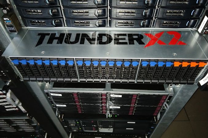
Yesterday during Marvell’s quarterly earnings call, the company had made a surprise announcement that they are planning to restructure their server processor development team towards fully custom solutions, abandoning plans for “off-the-shelf” product designs.
The relevant earning call statements are as follows:
"Very much aligned with our growing emphasis on custom solutions, we are evolving our ARM-based server processor efforts toward a custom engagement model.
[…]
Having worked with them for multiple generations, it has become apparent that the long-term opportunity is for ARM server processors customized to their specific use cases rather than the standard off-the-shelf products. The power of the ARM architecture has always been in its ability to be integrated into highly customized designs optimized for specific use cases, and we see hyperscale data center applications is no different. With our breadth of processor know-how and now our custom ASIC capability, Marvell is uniquely positioned to address this opportunity. The significant amount of unique ARM server processor IP and technology we have developed over the last few years is ideal to create the custom processors hyperscalers are requesting.
Therefore, we have decided to target future investments in the ARM server market exclusively on custom solutions. The business model will be similar to our ASIC and custom programs where customers contribute engineering and mask expenses through NRE for us to develop and produce products specifically for them. We believe that this is the best way for us to continue to drive the growing adoption of ARM-based compute within the server market."
We’ve had the opportunity to make a follow-up call with the teams at Marvell to get a little more background on the reasoning for such a move, given that only 6 months ago during the launch of the ThunderX3, the company had stated they were planning to ship products by the end of this year.
Effectively, as we’ve come to understand it, is that Marvell views the Arm server market at this moment in time to be purely concentrated around the big hyperscaler customers which have specific requirements in terms of their workloads, which require specific architecture optimisations.
Marvell sees the market beyond these hyperscaler customers to not be significant enough to be of sufficient value to engage in, and thus the company prefers to refocus their efforts in towards closer collaborations with hyperscaler costumers and fulfilling their needs.
The statement paints a relatively bleak view of the open Arm server market right now; in Marvell’s words, they do not rule out off-the-shelf products and designs in several years’ time when and if Arm servers become ubiquitous, but that currently is not the best financial strategy for the current ecoysystem. That’s quite a harsh view of the market and puts into question the ambitions of other Arm server vendors such as Ampere.
The company seemed very upbeat about the custom semicon design business, and they’re seemingly seeing large amounts of interest in the latest generation 5nm custom solutions they’re able to offer.
The company stated during the earning call that it still plans to ship the ThunderX3 by the end of this year, however it will only be available through customer specific engangements. Beyond that, it’s looking for custom opportunities for their hyperscaler customers.
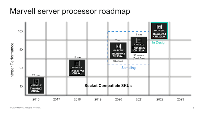
That also means we won't be seeing public availability for the dual-die TX3 product, and neither the in-design TX4 chip, which is unfortunate given that the company had presented their chip roadmap through 2022 only a few weeks ago at HotChips, which is now out of date / defunkt.
Although the company states that it’ll continue to leverage its custom IP for the future, I do wonder if the move has anything to do with Arm’s recent rise in the datacentre, and their very competitive Neoverse CPU microarchitectures and custom interconnects, essentially allowing anybody to design highly customizable products in-house, creating significant competition in the market.
From Marvell’s perspective, this all seems to make perfect sense as the company is simply readjusting towards where the money and maximum revenue growth opportunities lie. Having a hyperscaler win and keeping it is already a significant pie of the total market, and I think that’s what Marvell’s goal is here in the next several years.
Related Reading:
- Hot Chips 2020: Marvell Details ThunderX3 CPUs - Up to 60 Cores Per Die, 96 Dual-Die in 2021
- Hot Chips 2020 Live Blog: Marvell ThunderX3 (10:30am PT)
- Marvell Announces ThunderX3: 96 Cores & 384 Thread 3rd Gen Arm Server Processor
- Assessing Cavium's ThunderX2: The Arm Server Dream Realized At Last
- Marvell Unveils its Comprehensive Custom ASIC Offering
- Next Generation Arm Server: Ampere’s Altra 80-core N1 SoC for Hyperscalers against Rome and Xeon
- Ampere’s Product List: 80 Cores, up to 3.3 GHz at 250 W; 128 Core in Q4
- Amazon's Arm-based Graviton2 Against AMD and Intel: Comparing Cloud Compute
from AnandTech https://ift.tt/3hPKQde
via IFTTT
Intel confirms Marvel's Avengers Collector's Edition CPUs: cool packaging, but no game (updated)
https://ift.tt/2YKdrJF
")
Update (Aug 28): Marvel’s Avengers is set for release September 4 and if you were planning on buying the game or a new Intel-powered PC, take note that you can probably take advantage of Intel's gaming bundle. The offer runs from August 27 to February 28, 2021, redeemable until March 31,...

from TechSpot https://ift.tt/2EkPUYd
via IFTTT
Update (Aug 28): Marvel’s Avengers is set for release September 4 and if you were planning on buying the game or a new Intel-powered PC, take note that you can probably take advantage of Intel's gaming bundle. The offer runs from August 27 to February 28, 2021, redeemable until March 31,...
from TechSpot https://ift.tt/2EkPUYd
via IFTTT
Cryorig teases a 'New Generation' of CPU cooler
https://ift.tt/eA8V8J
Things are heating up in the heatsink market.
from Overclock3D.Net https://ift.tt/2G6CHU0
via IFTTT
Things are heating up in the heatsink market.
from Overclock3D.Net https://ift.tt/2G6CHU0
via IFTTT
Thursday 27 August 2020
TSMC Launches New N12e Process: FinFET at 0.4V for IoT
https://ift.tt/2G109St
from AnandTech https://ift.tt/3lonM7Q
via IFTTT

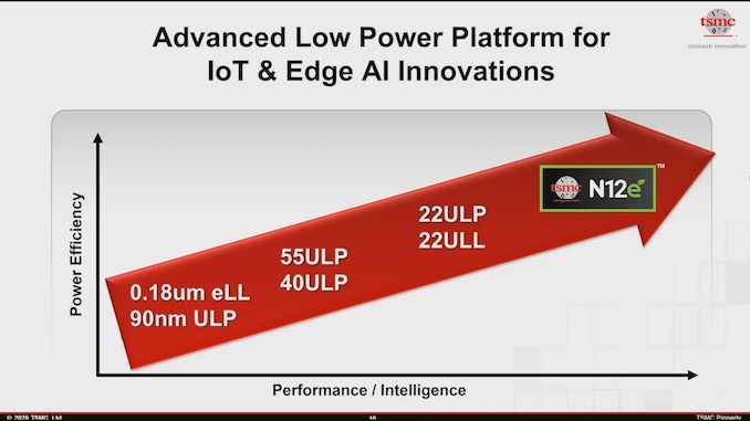
One of the main drivers for the semiconductor industry is the growth in always-connected devices that require silicon inside, either for compute, communication, or control. The ‘Internet of Things’ era, depending on who you speak to, is set to scale to many billions of devices and subsequently many billions of dollars in opportunities. In order to drive this segment, semiconductor foundries have been developing cost-effective low power process node technologies for its customers to help drive a new level of power efficiency and low cost implementations. TSMC’s newest process targeting this market was announced at its 2020 Technology Symposium, and is to be called N12e.
TSMC’s roadmap for its low powered platforms has centered around popular process node technologies optimized for low power and low leakage. Over the past decade TSMC has offered low power versions of 90nm, 55nm, 40nm and 22nm, with each generation giving smaller die areas and lower power, as well as other design optimizations specific to each need. These have all been planar technologies, however the new N12e process node is the next generation, and based on FinFETs.
FinFETs are, in a like-for-like scenario, more complex to build than planar transistors, and therefore should naturally cost more to produce. However, FinFET technologies also provide benefits in scaling and power, something this market is interested in. Rather than introduce FinFETs earlier in the cycle, TSMC has waited a few generations until it can deploy its most advanced FinFET designs to this market, to help ease the transition with the benefits that a most optimized design could bring.
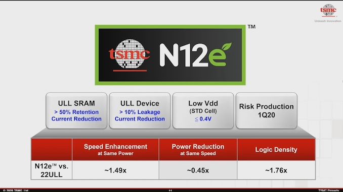
Within N12e compared to 22ULL, TSMC is promising a 1.49x increase in frequency at iso-power, or a 55% reduction in power at iso-speed. This also comes with a 1.76x increase in logic density, and a specialist low-voltage cell library capable of 0.4 volts. This extends the range of TSMC’s IoT process node offerings to a lower power bracket, as well as giving a better performance profile at all other powers as well.
N12e brings together technology from TSMC’s 16nm process and couples it with improvements and experience from 12FFC+, both of which have been used extensively in high performance computing. TSMC believes that integrating this with its ultra-low-leakage knowledge will help enable the next generation of 5G-enabled IoT Edge devices, by providing low power routes to AI accelerators for speech recognition, health monitoring and machine vision.
The main competitor to N12e would be GlobalFoundries 12FDX platform, which is built on GF’s 12nm FD-SOI technology, with claims of better power consumption and lower cost than equivalent FinFET designs. However despite talk of 12 FDX for several years (and news of new MRAM support and such), there have been no public design wins for the process.
It is unclear when TSMC will start taking orders for its N12e platform, however the company has said it is ‘excited’ for the next generation of products built on it.
Source: TSMC N12e
Related Reading
- TSMC Details 3nm Process Technology: Full Node Scaling for 2H22 Volume Production
- TSMC To Build 5nm Fab In Arizona, Set To Come Online In 2024
- TSMC & Broadcom Develop 1,700 mm2 CoWoS Interposer: 2X Larger Than Reticles
- TSMC Boosts CapEx by $1 Billion, Expects N5 Node to Be Major Success
- Early TSMC 5nm Test Chip Yields 80%, HVM Coming in H1 2020
- TSMC: 5nm on Track for Q2 2020 HVM, Will Ramp Faster Than 7nm
- TSMC: N7+ EUV Process Technology in High Volume, 6nm (N6) Coming Soon
- GlobalFoundries' 22FDX with MRAM is Ready
- GlobalFoundries Announces 22FDX Milestone: $2 Billion in Design Wins


from AnandTech https://ift.tt/3lonM7Q
via IFTTT
TSMC: We have 50% of All EUV Installations, 60% Wafer Capacity
https://images.anandtech.com/doci/16042/Manufacturing%20Excellence.mkv_snapshot_02.54_[2020.08.25_14.16.25]_575px.jpg
from AnandTech https://ift.tt/2YCO0JO
via IFTTT
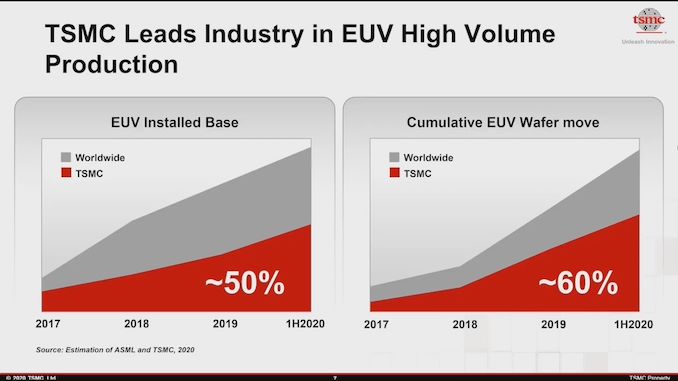
One of the overriding central messages to TSMC’s Technology Symposium this week is that the company is a world leader in semiconductor manufacturing, especially at the leading edge process technology. To further hit the message home, TSMC showcased a slide indicating where it stands in relation to others: by using a combination of public ASML statements and their own internal purchase sheets, TSMC predicts that they have ~50% of all the active EUV machines installed worldwide. Beyond that, the company also has a number of ~60% for cumulative EUV wafer production.
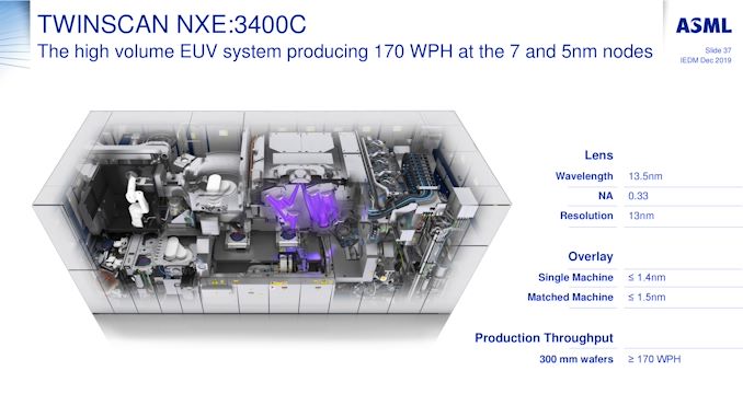
Current known public EUV processes from the big fabs include TSMC’s 7+ and N5, as well as Samsung’s 7LPP (and anything below), with Intel’s EUV efforts only entering in its own 7nm portfolio next year. Anything beyond these processes at the leading edge will continue to extend EUV use. EUV machines typically have a lower throughput, anywhere from 120-175 wafers per hour, than regular DUV machines which can reach 275 wph on the latest versions, however since 1 layer of EUV typically replaces 3-4 layers of DUV, the throughput is higher, but nonetheless the desire to scale out to multiple EUV machines to increase the physical number of wafers is a keen target for these foundries.
The only company that makes EUV machines is ASML, and the company publically announces how many machines it sells each year. The details are as follows:
| ASML's EUV Shipments | ||||||||||||||||||
| 2015 | 2016 | 2017 | 2018 | 2019 | 2020 | 2021 | ||||||||||||
| Actual | 2 | 4 | 10 | 3 | 4 | 5 | 6 | 4 | 7 | 7 | 8 | 2 | 9 | - | - | - | ||
| Target | - | - | - | 20 | 30 | 35 | 45-50 | |||||||||||
| 2018 and beyond is split per quarter for actual shipped numbers Data taken from ASML's Financial Reports |
||||||||||||||||||
Note that each year so far, ASML hasn’t quite hit its targets, but has done near enough, although sales in Q1 2020 were lower than I would expect, indicating that by end of Q2 2020, ASML has only shipped 13 out of the proposed 35 systems. These numbers include all the different types of Twinscan NXE machines that ASML has built, with the more recent ones having better throughput (and sometimes the older ones get retrofitted). As of the end of Q2 2020, we predict that ASML has shipped around 71 of these EUV machines, and will likely hit 90 by the end of 2020. Some observers have noted that ASML may have a backlog of as many as 49 EUV scanner orders, even with these shipment targets.
If ASML has shipped 71 machines, that would mean, according to TSMC’s numbers, the company has around 30-35. Note that TSMC’s numbers are for ‘Installed EUV’ machines – we learned from our trip to GlobalFoundries in Q1 2018 that it takes up to 6 months from getting the parts to calibrating the machine for use. At present, some of these foundries therefore have EUV machines sitting around waiting to be installed, or in the case of Intel, perhaps only in use for early testing or pre-risk trials. We know that GlobalFoundries had two early EUV machines, installed one, but ended up selling both when it decided not to pursue leading edge 7nm, and SMIC ordered one but as far as we know it wasn’t installed due to restrictions imposed by the US.
As TSMC grows its Fab 18 for N5 production, and ramps its EUV integration, it will be interesting to see if TSMC is ever limited by the number of machines it has. At some point Intel is going to want to buy a number when it deploys its 7nm processes (I’ve seen predictions that Intel has at least ~10 machines already, but I can’t confirm that) as well, so there might be a tussle for who gets their order delivered first.
One thing is for sure however, ASML is sitting pretty right in the middle with a monopoly on everything. I still have an invite to visit one of their EUV machine factories in Connecticut, which when the COVID mess is all over I intend to follow up on. It should be exciting.
Related Reading
- SMIC Details Its N+1 Process Technology: 7nm Performance in China
- GlobalFoundries Stops All 7nm Development: Opts To Focus on Specialized Processes
- Intel 7nm Delayed By 6 Months; Company to Take “Pragmatic” Approach in Using Third-Party Fabs
- TSMC: N7+ EUV Process Technology in High Volume, 6nm (N6) Coming Soon
- TSMC: 3nm EUV Development Progress Going Well, Early Customers Engaged
- TSMC’s 5nm EUV Making Progress: PDK, DRM, EDA Tools, 3rd Party IP Ready
- ASML’s First Multi-Beam Inspection Tool for 5nm
- TSMC Expects 5nm to be 11% of 2020 Wafer Production (sub 16nm)
- ‘Better Yield on 5nm than 7nm’: TSMC Update on Defect Rates for N5
- TSMC Details 3nm Process Technology: Full Node Scaling for 2H22 Volume Production
- TSMC Confirms Halt to Huawei Shipments In September
from AnandTech https://ift.tt/2YCO0JO
via IFTTT
Wednesday 26 August 2020
Where are my GAA-FETs? TSMC to Stay with FinFET for 3nm
https://ift.tt/3hx9kIb
from AnandTech https://ift.tt/2YB4ane
via IFTTT
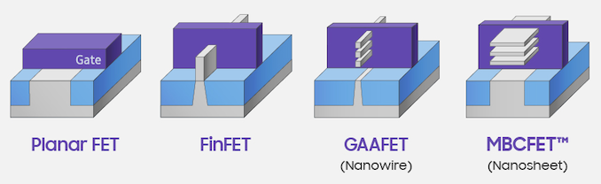
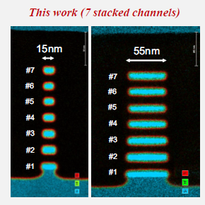
As we passed that 22nm to 16nm barrier, almost all the major semiconductor fabrication companies on the leading edge transitioned from planar resistors to FinFET transistors. The benefits of FinFET were numerous, including better drive currents and lower leakage, better scalability, faster switching times, and an overall better transistor of choice for semiconductor logic. With FinFETs, and multiple rounds of improvements, the technology has scaled from Intel’s first 22nm products down to the 5nm products we will see from TSMC’s partners this year.
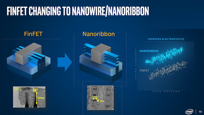
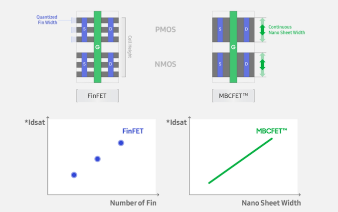
As expected, at some point the ability to scale a FinFET will become prohibitive, and new technologies will be needed to help continue the scaling. Research on post-FinFET transistor technology has been progressing at a break-neck pace, and most attention has been moved into ‘Gate-All-Around’ technology, which lifts the channel and allows the channel width to scale as needed for the type of transistor in use. GAA-FETs offer significant advantages when it comes to transistor performance control – for most FinFET processes, foundries can offer several designs based on voltage and performance, but GAA-FET designs turn those discrete options into something more continuous. You might see these referred to as nanosheets, or nanowires.
From Samsung
As is perhaps to be expected, GAA-FET designs (and layered GAA-FETs) are more complex to build than FinFETs or planar transistors. The first GAA-FET demonstration was in 1986, and in 2006 a 3nm implementation was demonstrated. However, building it in a lab compared to building it at scale as part of a foundry process available to customers is a different scale of complexity. At a number of technical semiconductor conferences through 2018 and 2019, a number of design companies and foundry offerings have discussed GAA-FET or similar designs as part of their upcoming portfolio.
Most notably, Intel has mentioned that they will start using it within the next 5 years, which would put it around its 5nm-3nm node technologies.
Intel
Samsung has announced its intention to deliver its version, known as MBC-FETs, as part of its 3nm process node, expected to be in volume manufacturing by late 2021. In May 2019, the company released a statement that the first v0.1 version of its 3GAE PDK was ready for customers. Over a year later, we would expect this to be on track – the 2020 version of Samsung’s Foundry Forum, which was delayed due to COVID, should be happening later this year.
Samsung
As these sorts of transistors grow in use, we expect the range of sheet widths available to increase, as well as the number of stacked layers in a GAA design. CEA-Leti this year, at the 2020 Symposia on VLSI Technology and Circuits, demonstrated a 7-layer GAA-FET using nanosheets specifically for high-performance computing.
CEA-Leti
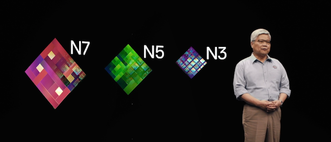
So what has happened with TSMC? As part of the Technology Symposium, it has stated that for its 3nm process technology it will remain with FinFETs. The company states that it has enabled a significant update to its FinFET technology to allow performance and leakage scaling through another iteration of its process node technology. TSMC’s N3 will use an extended and improved version on FinFET in order to extract additional PPA - up to 50% performance gain, up to 30% power reduction, and 1.7x density gain over N5. TSMC stated the predictability of FinFETs will help enable the company deliver the technology on an approved timescale.
This last statement is more than telling – if the development of FinFETs, now on its 3rd/4th/5th generation (depending on the foundry), has enabled a level of comfort and predictability that a first generation of GAA-FET cannot provide, then in order to satisfy its big customers (almost all leading-edge logic silicon), it has to keep to its cadence. That being said, there could be a chance for TSMC to offer GAA-FETs on different versions of its 3nm nodes in the future if it wishes, however the company has not made any public statements at this time to this effect, compared to Intel and Samsung.

As always with these technologies, the goal is to scale and bring some reality to wherever Moore’s Law is going. TSMC’s customers will have to wait until later to see if GAA-FETs can bring a more optimized flavor of performance to the table.
Related Reading
- TSMC Details 3nm Process Technology: Full Node Scaling for 2H22 Volume Production
- TSMC To Build 5nm Fab In Arizona, Set To Come Online In 2024
- TSMC & Broadcom Develop 1,700 mm2 CoWoS Interposer: 2X Larger Than Reticles
- TSMC Boosts CapEx by $1 Billion, Expects N5 Node to Be Major Success
- Early TSMC 5nm Test Chip Yields 80%, HVM Coming in H1 2020
- TSMC: 5nm on Track for Q2 2020 HVM, Will Ramp Faster Than 7nm
- TSMC: N7+ EUV Process Technology in High Volume, 6nm (N6) Coming Soon
from AnandTech https://ift.tt/2YB4ane
via IFTTT
Tuesday 25 August 2020
TSMC Expects 5nm to be 11% of 2020 Wafer Production (sub 16nm)
https://ift.tt/31siEaL
from AnandTech https://ift.tt/3lhiydZ
via IFTTT
One of the measures of how quickly a new process node gains traction is by comparing how many wafers are in production, especially as that new process node goes through risk production and then into high volume manufacturing. You can tell a lot about how much confidence a foundry has in its new process by looking at the number of wafers in production, as well as the expected range of customers and products that are set to be produced. As part of TSMC’s Technology Symposium 2020, we were treated to a little insight into the growth of its new 5nm process technology.
TSMC’s 5nm process, or strictly speaking its first production version of 5nm, known as N5, is currently in the process of high volume manufacturing. We are expecting the first consumer products that use N5 processors, particularly smartphones, out by the end of the year. That means that the companies who are building those products have already worked with pre-production silicon for validation, put their orders in for N5 parts, and may already be getting the first deliveries of the new hardware.
With such a new process, we always expect that initial production, even in ‘high volume production’ mode, is usually slow. This is due to product development, but also extensive validation and to make sure that the product isn’t a dud (such as TSMC’s ill-fated 20nm process). However, judging by the slides produced by TSMC at its Technology Symposium, it looks like that 11% of its 2020 production of 16nm+ wafers will be on 5nm.
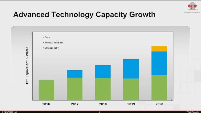
It should be noted that this graph has ’12-inch wafer equivalents’ as the y-axis, which means that if any process node would use 8-inch wafers, it would be scaled accordingly. However, all of these leading edge process nodes are likely to be on 12-inch wafers.
Unfortunately there’s no real sense of how many wafers that is. TSMC has stated in another slide that it produced over 12 million 12-inch wafer equivalents in 2019, but that covers all processes and all facilities. At financial disclosures, TSMC does a breakdown of each node, but only in terms of revenue.
However, comparing 5nm to TSMC’s 7nm capability, it does show that 2019 to 2020, 7nm increased by 22.7%, and in 2020, 5nm production will be ~24% of 7nm production. This leads into TSMC’s narrative that it expects to grow its 5nm production to double in 2021, and triple in 2022, using the 2020 numbers as a base.
TSMC did give some insight into its 5nm manufacturing facilities also.
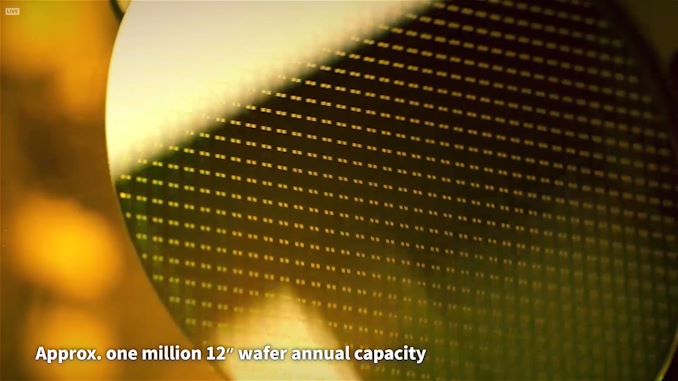
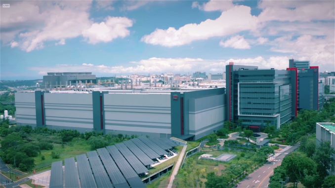
All of TSMC’s 5nm chips are being built at TSMC’s Fab 18, the newest fabrication plant that spreads over six buildings, which TSMC calls its ‘fourth GigaFab’. Fab 18 broke ground on January 26th 2018, and a year later the company started installing over 1300 manufacturing tools, including EUV machines, in a process that only took 8 months. From there, the company started testing its 5nm risk production, and started high-volume manufacturing in Q2. TSMC states that Fab 18 is capable of producing over one million 12-inch wafers per year, all on 5nm, and claims it leads the industry in energy efficiency for a fab of it size.
Related Reading
- TSMC Details 3nm Process Technology: Full Node Scaling for 2H22 Volume Production
- TSMC To Build 5nm Fab In Arizona, Set To Come Online In 2024
- TSMC & Broadcom Develop 1,700 mm2 CoWoS Interposer: 2X Larger Than Reticles
- TSMC Boosts CapEx by $1 Billion, Expects N5 Node to Be Major Success
- Early TSMC 5nm Test Chip Yields 80%, HVM Coming in H1 2020
- TSMC: 5nm on Track for Q2 2020 HVM, Will Ramp Faster Than 7nm
- TSMC: N7+ EUV Process Technology in High Volume, 6nm (N6) Coming Soon


from AnandTech https://ift.tt/3lhiydZ
via IFTTT
Subscribe to:
Posts (Atom)