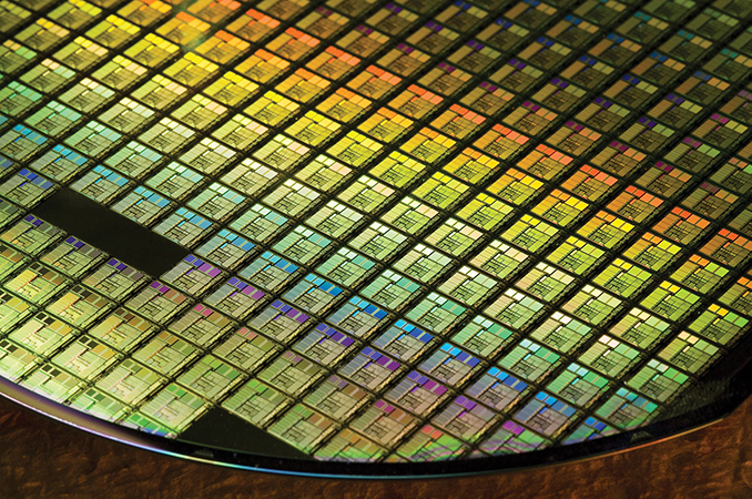
TSMC last week announced that it had started high volume production (HVM) of chips using their first-gen 7 nm (CLN7FF) process technology. The contract maker of semiconductors says it has over a dozen of customers with tens of designs eager to use the technology to make their integrated circuits.
The 7 nm node is a big deal for the foundry industry in general and TSMC in particular. When compared to the CLN16FF+ technology (TSMC’s most widely used FinFET process technology) the CLN7FF will enable chip designers to shrink their die sizes by 70% (at the same transistor count), drop power consumption by 60%, or increase frequency by 30% (at the same complexity). So far, TSMC has taped out 18 customer products using the CLN7FF technology, more than 50 CLN7FF products will be taped out by the end of 2018.
Unlike TSMC’s CLN10FF, which is used by a limited number of customers for a limited number of mobile SoCs, the CLN7FF is expected to be used to build CPUs, GPUs, FPGAs, neural network processors, cryptocurrency mining accelerators, mobile SoCs and so on. This is important because demand for smartphones is slowing down and TSMC needs other customers to offset lower orders for mobile SoCs.
“So far, we have already favored out more than 18 customer products with good yield [and] performance,” said C. C. Wei, a Co-CEO and President of TSMC, during a conference call with financial analysts. “More than 50 products tape-outs has been planned by end of this year from applications across mobile, server CPU, network processor, gaming, GPU, PGA, cryptocurrency, automotive and AI. Our 7nm is already in volume production.”
TSMC’s CLN7FF process technology will rely on deep ultraviolet (DUV) lithography with argon fluoride (ArF) excimer lasers operating on a 193 nm wavelength. As a result, the world’s largest contract maker of semiconductors will be able to use existing manufacturing tools to make 7 nm chips. Meanwhile, to keep using DUV lithography the company and its customers have to use multipatterning (triple and quadruple patterning), which increases design and production costs as well as product cycles.
| Advertised PPA Improvements of New Process Technologies Data announced by companies during conference calls, press briefings and in press releases |
|||||||
| TSMC | |||||||
| 16FF+ vs 20SOC |
10FF vs 16FF+ |
7FF vs 16FF+ |
7FF vs 10FF |
7FF+ vs 7FF |
|||
| Power | 60% | 40% | 60% | <40% | 10% | ||
| Performance | 40% | 20% | 30% | ? | higher | ||
| Area Reduction | none | >50% | 70% | >37% | ~17% | ||
Next year TSMC intends to introduce its first manufacturing tech that will use extreme ultraviolet lithography (EUVL) for select layers. The CLN7FF+ will be the company’s second-generation 7 nm fabrication process because of design rules compatibility and because it will keep using DUV tools that TSMC uses today for its CLN7FF production. From a general PPA (power, performance, area) improvement point of view, TSMC expects its CLN7FF+ to offer a 20% higher transistor density and a 10% lower power consumption at the same complexity and frequency when compared to the CLN7FF. Furthermore, TSMC’s EUV-based 7 nm technology could also feature higher performance and a tighter distribution of currents, but the company’s execs do not quantitate the improvements just now.
“Our N7+ silicon result today are very encouraging,” said Mr. Wei. “Not only we have demonstrated equivalent or better performance [and] yield on both 256 Mb SRAM and on product like test vehicle when compared to [the] N7 baseline, we have also demonstrated a tighter distribution of electrical parameters in the areas, where EUV is supplied.”
TSMC is on track to start HVM using its 7 nm EUV process technology in mid-2019. Going forward, the company will increase usage of ASML’s Twinscan NXE step and scan systems when it starts to process wafers using its CLN5 (5 nm) process technology in 2020. According to the co-CEO of TSMC, the EUV results have been encouraging so far: the company’s 256 Mb SRAM test chip is already made with a “consistent double-digit yield”, which is rather good for a technology that is two years away from HVM. The high-ranking executive of TSMC also noted that the EUV infrastructure in general has made a good progress in the recent quarters. In particular, the company observed lower pellicle defects, higher mask yields, and improved photoresists.
Related Reading:
- Samsung and TSMC Roadmaps: 8 and 6 nm Added, Looking at 22ULP and 12FFC
- TSMC Teams Up with ARM and Cadence to Build 7nm Data Center Test Chips in Q1 2018
- GlobalFoundries Details 7 nm Plans: Three Generations, 700 mm², HVM in 2018
- The Future of Silicon: An Exclusive Interview with Dr. Gary Patton, CTO of GlobalFoundries
from AnandTech https://ift.tt/2Jo4tHR
via IFTTT
No comments:
Post a Comment