This year at IFA, instead of suddenly finding the new silicon on the show floor, Huawei’s CEO Richard Yu announced this year’s new Kirin 980 during the company’s keynote speech. For readers who’ve been attentively following our articles over the last few months, today’s news should hopefully not come at too big of a surprise, as I’ve been heavily hinting at the timing of the first new 7nm Cortex A76 silicon designs coming later this year in commercial devices, with HiSilicon being the prime candidate for being the first vendor on the market with the their new generation SoC.
Huawei’s silicon design division HiSilicon has been a key strategic component for the company’s products, as it enables it to differentiate itself in a more drastic way than what we usually see from other vendors who simply rely on established open-market SoC vendors such as Qualcomm. This kind of strategy of course is a double-edged sword, as if you’re all-in with your in-house silicon, it also means that these designs must be executed properly, as otherwise you find yourself in an unfavourable competitive position.
The Kirin 950 was an impressive chip as it boasted the first Cortex A72 design on a then new TSMC 16FF manufacturing process – this paid off plenty for Huawei as the combination of new IP as a new manufacturing node resulted in a very competitive silicon which directly translated into favourable characteristics of the handsets in that it was used in.
The Kirin 960 and Kirin 970 on the other hand showcased the risky side of this strategy, and where things can go off-track – the Kirin 960 was a 16nm SoC released in a device generation where 10nm competitors such as the Snapdragon 835 and Exynos 8895 dominated. The Kirin 970 fared better when switching to a 10nm manufacturing node, but this time around HiSilicon wasn’t able to include the newest Arm CPU IP, relying on an A73 CPU while the Snapdragon 845 embraced the new A75. Furthermore the last two Kirin generations had showcased extremely uncompetitive GPU performance and efficiency figures – here HiSilicon is stuck and is at the whim of IP vendors’ ability to produce competitive designs against market leaders such as Qualcomm.
The reason as to why I reiterated what happened to the last few generations, is that this time around HiSilicon finds itself in a very favourable position where IP and manufacturing is aligned into what is essentially a best-case scenario for the new design. Arm’s new Cortex A76 and Mali G76 both promise great leaps in terms of performance and power efficiency, and TSMC is in mass production of its new 7nm manufacturing node.
Today we present the new Kirin 980, the first announced TSMC 7nm SoC as well as the first Cortex A76 and Mali G76 design:
| HiSilicon High-End Kirin SoC Lineup | |||
| SoC | Kirin 980 | Kirin 970 | Kirin 960 |
| CPU | 2x A76 @ 2.60 GHz 2x A76 @ 1.92 GHz @ 512KB L2's 4x A55 @ 1.80 GHz @ 128KB L2's 4MB DSU L3 |
4x A73 @ 2.36 GHz 4x A53 @ 1.84 GHz 2MB L2 |
4x A73 @ 2.36GHz 4x A53 @ 1.84GHz 2MB L2 |
| GPU | ARM Mali-G76MP10 @ 720 MHz |
ARM Mali-G72MP12 @ 746 MHz |
ARM Mali-G71MP8 @ 1037MHz |
| LPDDR4 Memory |
4x 16-bit CH LPDDR4X @ 2133MHz 34.1GB/s |
4x 16-bit CH LPDDR4X @ 1833 MHz 29.9GB/s |
4x 16-bit CH LPDDR4 @ 1866MHz 29.9GB/s |
| Storage I/F | UFS 2.1 | UFS 2.1 | UFS 2.1 |
| ISP/Camera | New Dual ISP +46% speed |
Dual 14-bit ISP | Dual 14-bit ISP (Improved) |
| Encode/Decode | 2160p60 Decode 2160p?? Encode |
2160p60 Decode 2160p30 Encode |
1080p H.264 Decode & Encode 2160p30 HEVC Decode |
| Integrated Modem | Kirin 980 Integrated LTE (Category 21/18) DL = 1400 Mbps 4x4 MIMO 3x20MHz CA, 256-QAM (5CA no MIMO) UL = 200 Mbps 2x2 MIMO 1x20MHz CA, 256-QAM |
Kirin 970 Integrated LTE (Category 18/13) DL = 1200 Mbps 5x20MHz CA, 256-QAM UL = 150 Mbps 2x20MHz CA, 64-QAM |
Kirin 960 Integrated LTE (Category 12/13) DL = 600Mbps 4x20MHz CA, 64-QAM UL = 150Mbps 2x20MHz CA, 64-QAM |
| Sensor Hub | i8 | i7 | i6 |
| NPU | Dual @ >2x perf | Yes | No |
| Mfc. Process | TSMC 7nm | TSMC 10nm | TSMC 16nm FFC |
The new Kirin 980 checks off all of the newest available IPs from Arm, finally employing a new DynamIQ CPU cluster configuration comprised of 4 Cortex A76's and 4 Cortex A55s.
The biggest surprise to today’s announcement for me is to see that HiSilicon has made the step forward to fully take advantage of Arm’s new DSU cluster and its asynchronous CPU configuration, and actually implement the brand new Cortex A76 into two groups, each housed in their own clock and voltage plane.
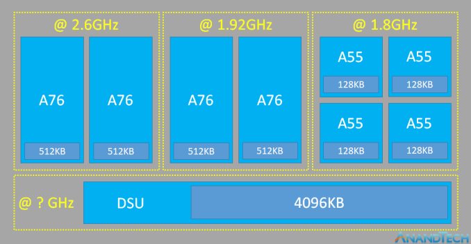
The highest performance Cortex A76 pair runs at up to 2.6GHz. This is less than Arm’s originally announced 3GHz target for the CPU, however I had warned readers to expect more conservative clocks around the 2.5GHz figure, as the higher clock rates seemingly were meant for higher TDP form-factors. Nevertheless, the new CPU microarchitecture still brings with it substantial performance improvements, and thus will still perform very well at 2.6GHz, posting leading performance for this generation.
The surprise of seeing the second pair of Cortex A76 cores running at up to 1.92GHz is actually quite fantastic news for power efficiency. Here we see HiSilicon include what is essentially a “medium” efficiency group of CPUs. Because these two cores are running on a separate clock and voltage plane to the primary performance A76 pair, it means they can operate at different efficiency points, enabling more effective power savings in varied multi-threaded operation.
Previously, quad-core clusters were running on the same clock and voltages, and if there was a single high performance thread requiring a high performance state, it meant that other medium-performance threads were forced to take a power efficiency penalty by needlessly running at this less efficient performance state. By introducing a mid-tier, this effectively eliminates such kind of overhead which is commonly found in real-world applications.
I haven’t been able to confirm this with HiSilicon as of yet, but the reduced clock of this mid pair of A76 would also strongly point out to a possibly different physical implementation with a lower silicon sign-off frequency. This means that even though both pairs of A76’s are the same IP, this mid-pair are very likely to actually be more efficient when running at the same frequency.
Finally, we see four new Cortex A55 cores as the most power-efficient workhorses of the SoC who’ll be able to take the brunt of workloads, running at up to 1.8GHz. Here again, virtue of the mid-performance cluster, HiSilicon is likely able to implement a very power-efficiency focused physical implementation for the A55’s, resulting in clock speeds that in range with current generation A53 and A55 SoCs.
Cache wise, all the Cortex A76’s come with their recommended 512KB L2 cache configurations while the A55’s employ 128KB caches. As a reminder, in the new DynamIQ cluster configuration, the L2 caches for these designs are private to each CPU core. The L3 cache in the DSU has seen a full implementation at 4MB, double that of what we’ve seen in the Snapdragon 845.
I haven’t been able to confirm the frequency of the DSU in the Kirin 980, nor if it actually has a separate clock and voltage plane of its own, here it might be possible that it’s could be on the same plane with the A55’s. Again, that’s just speculation on my part, the other possibility is that we have 4 full clock and voltage planes for the whole CPU complex.
75% higher CPU performance, 58% better efficiency compared to Kirin 970
In terms of performance gains, HiSilicon promises 75% gains over the Kirin 970, which after a bit of math actually ends up basically exactly where I had projected the A76 to land, based on Arm’s own performance claims.
The following projection is of my own, and takes into account both Arm’s and HiSilicon’s matching performance claims:
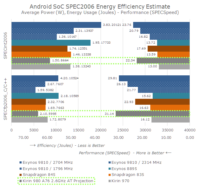
As you may have noted, the power and efficiency estimates are also included. HiSilicon proclaims that the Kirin 980 is 58% more power efficient than the Kirin 970. We haven’t been able to clarify if this means that the perf/W is 58% better at the same performance of the 970, or if the Kirin 980 has a 58% better perf/W at both SoC’s respective peak performance states. The projection assumes the latter, and it actually again it matches up with Arm’s own claims about the Cortex A76.
I’m still very very sceptical about these numbers as they seem quite fantastic; yet to date I haven’t seen any contradictory information that would actually rebuke these estimates. For the time being, until we actually get our hands on the first Kirin 980 device, take the above power and efficiency estimate with a large grain of salt.
The move to a 3-tier CPU hierarchy also brings with itself complications in terms of scheduling. As we’ve seen this year, scheduling is very much a new critical component of modern SoCs as with the very high dynamic range of performance and power, using the most optimal solution is critical in extracting the best out of the silicon. Here HiSilicon promises a new “Flexible scheduling” mechanism. We unfortunately don’t have any more details on this, but it’s going to be a crucial component of the new Kirin 980.
New Mali G76MP10 – Actually 20 "rendering pipelines"
Moving on, the Kirin 980 is also the first SoC to employ Arm’s new generation Mali G76 GPU. The G76 greatly differs from past Midgard and Bifrost GPUs in that it vastly changes the block structure inside what you consider a “core”. Here the G76 essentially doubled up on texture units, render units, and doubles the width of the arithmetic pipelines. In effect, a G76 core is pretty much equivalent to two G72 cores.
What this means that while on paper the G76MP10 might at first glance looks smaller than the G72MP12 in the Kirin 970, yet it actually represents a 66% increase in the computational resources, not taking into account microarchitectural improvements of the new IP.
The Kirin 970’s GPU was clocked at up to 747MHz – however the power draw at this frequency was still too great for the SoC to handle, resulting in real-world workloads effectively running at much lower frequencies.
The Kirin 980 runs the new GPU at 720MHz and promises a 46% performance boost. We didn’t have any clarification of the workload here, but generally the industry standard is usually GFXBench Manhattan.
46% higher performance, and *178%* higher power efficiency
Now the real kicker of the new GPU, is that HiSilicon proclaims a massive 178% boost in power efficiency when compared to the Kirin 970. Putting these claims into our efficiency table and extrapolating the results:
| GFXBench Manhattan 3.1 Offscreen Power Efficiency (System Active Power) |
||||
| Mfc. Process | FPS | Avg. Power (W) |
Perf/W Efficiency |
|
| Kirin 980 Projection Based on +% | 7FF | 55 ? | 3.5 ? | 16 fps/W ? |
| Galaxy S9+ (Snapdragon 845) | 10LPP | 61.16 | 5.01 | 11.99 fps/W |
| Galaxy S9 (Exynos 9810) | 10LPP | 46.04 | 4.08 | 11.28 fps/W |
| Galaxy S8 (Snapdragon 835) | 10LPE | 38.90 | 3.79 | 10.26 fps/W |
| LeEco Le Pro3 (Snapdragon 821) | 14LPP | 33.04 | 4.18 | 7.90 fps/W |
| Galaxy S7 (Snapdragon 820) | 14LPP | 30.98 | 3.98 | 7.78 fps/W |
| Huawei Mate 10 (Kirin 970) | 10FF | 37.66 | 6.33 | 5.94 fps/W |
| Galaxy S8 (Exynos 8895) | 10LPE | 42.49 | 7.35 | 5.78 fps/W |
| Galaxy S7 (Exynos 8890) | 14LPP | 29.41 | 5.95 | 4.94 fps/W |
| Meizu PRO 5 (Exynos 7420) | 14LPE | 14.45 | 3.47 | 4.16 fps/W |
| Nexus 6P (Snapdragon 810 v2.1) | 20Soc | 21.94 | 5.44 | 4.03 fps/W |
| Huawei Mate 8 (Kirin 950) | 16FF+ | 10.37 | 2.75 | 3.77 fps/W |
| Huawei Mate 9 (Kirin 960) | 16FFC | 32.49 | 8.63 | 3.77 fps/W |
| Huawei P9 (Kirin 955) | 16FF+ | 10.59 | 2.98 | 3.55 fps/W |
The proclaimed performance boost would still be a tad too low catch up to the Snapdragon 845’s Adreno 630, at least in this workload. Here depending on how the Mali G76 scales, we might have different results based on different tests, showing a rebalancing of fillrate heavy workloads versus arithmetic/compute heavy workloads.
Where the Kirin 980 would showcase a large jump is in power consumption and efficiency. Again, HiSilicon’s marketing claims here end up matching what we had projected for the G76, based on Arm’s own figures. If this ends up as expected in measured devices, it would mean that the new Kirin would finally get back to sustainable power levels of that of the Kirin 950, shedding away the awful legacy of the first two Bifrost generation GPUs.
I’ve been banging the drums of the problem of sustainable performance a lot this year, and I do really hope the Kirin 980 ends up near the projections, because that would be a significant step forward for not only the SoC, but general consumer experience as well.
Faster memory controller
The new chipset sports an LPDDR4X memory controller, although it’s able to claim to be the industry’s first one to run at 2133MHz, resulting in a 13% increase in bandwidth. One of the weaknesses of the Kirin 970 was a memory controller that was quite power hungry at higher frequencies, here’s to hoping that the new design resolves these issues and we see better efficiency at high performance states.
Surprisingly, HiSilicon disclosed some memory latency and bandwidth figures: In the GeekBench 4 tests the Kirin 980 measures 138ns versus a quoted 176ns for the Snapdragon 845. This actually was a bit eye-brow raising as in context, the latency figure isn’t all that good: the Kirin 970 sported a similar 138ns latency as well, coming in the same ballpark of the Snapdragon 835. Yet all are worse than the Exynos 9810’s 78ns figure. Here I do hope the non-improvement doesn’t limit the peak performance of the A76 in the same way Qualcomm’s added latency of their new L4 system cache in the S845 hindered the A75 core’s performance.
Bandwidth figures are quoted at 23.1GB/s versus 19.2GB/s for the Snapdragon 845. I’ve been told GB4’s memory bandwidth test has issues scaling up after a certain point, so I’m not putting too much weight on these results for the time being.
New ISP with imaging features
The Kirin 980 sports a new ISP that increases is processing throughput capability by up to 46%, able support higher resolution camera streams. A first for HiSilicon is the introduction of a 10-bit pipeline for HDR capture, a feature also introduced in this year's competing SoCs, however only seldom used in practise due to colour management and displays lagging behind in terms of adoption.
The new ISP is able to now use “multi-pass noise reduction”, which sound much like the multi-frame noise reduction features introduced in the Snapdragon 845 this year, where noise reduction is not perform on a spatial pixel basis, but on a temporal inter-frame basis, resulting in sharper noise-free images without the side-effect of blurring. There’s also a new video encoding pipeline which promises “33% shorter delay” between captures. This last part was quite unclear in its meaning – the Kirin 970 lacked 4K60 encoding capabilities, and whether the Kirin supports it is something we still need to clarify with the company.
New “Dual-NPU” at 2x the throughput
The Kirin 980 continues improving its neural network inference acceleration IP, and introduces a new “Dual NPU”. In fact what this means is that the block essentially has been doubled up in the same way you would add a scaling unit to a GPU. The block still only handles one model kernel at a time, meaning in effect the speed of a single inference should be doubled, depending on NN model of course.
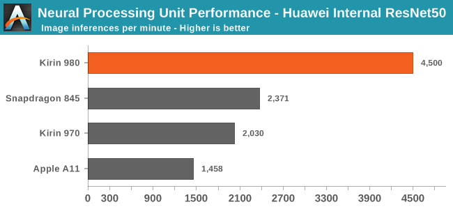
The new unit is said to be ~2.2x faster than the Kirin 970’s NPU, achieving up to 4500 inferences per minute, or 75 fps in their in-house test. They present figures for the Snapdragon 845 and Apple A11 as well, and as far as I can tell based on my own testing, these are very much accurate in terms of the observed performance.
Faster Category 21 Integrated Modem up to 1400Mbps
The new modem in the Kirin 980 elevates the capabilities of the predecessor – now it’s able to support up to UE Cat 21 download speeds of up to 1400Mpbs. This is achieved of up to 3x carrier aggregation in combination of 4x4 MIMO, all while support 2x2 MIMO and new 256-QAM in the upload link (Category 18), and achieving 200Mbps upload speeds.
6.9bn transistors on <100mm² thanks to TSMC’s new 7nm manufacturing node
The new chipset boasts 6.9bn transistors – an increase of 25% compared to last year’s Kirin 970 coming in at 5.5bn. HiSilicon was able to maintain a small die area of less than 100mm² thanks to the new 7nm TSMC process node. The project started in 2015 with 7nm process node research, with IP block unit development starting in 2016 and validation happening in 2017. Finally the SoC has been in mass production since this summer.
In-house WiFi Chipset
As surprise side-announcement was the reveal of the new Hi1103 WiFi chipset. The new chip supports 802.11ac with up to 1732Mbps speeds and 2x2 MIMO of up to 160MHz wide channels. I say that this is surprising because usually Huawei fell back to Broadcom BCM WiFi solutions which are considered to be industry leading and essentially found in every flagship device on the market. It’ll be interesting to see how the new HiSilicon chipset performs in comparison.
All the planets seem aligned for the Kirin 980
The Kirin 980 really does look like it’s on its way to be an exceptionally well balanced SoC with major improvements in every regard. The Kirin 960 and 970 had a rough time competing, both due to a process node disadvantage and then an IP disadvantage. Both suffered a lot from bad GPU performance and efficiency. Here the Kirin 980 looks to resolve these issues and the combination of Arm’s new Cortex A76 CPU cores, G76 GPU, new internal IP blocks such as memory controller, ISP and updated NPU, combined with a new leading-edge 7nm manufacturing process. The combination of all these new characteristics put the new Kirin 980 in an excellent competitive position, and the upcoming Mate 20 should be a device to look forward to.
Related Reading
- HiSilicon Kirin 970 - Android SoC Power & Performance Overview
- HiSilicon Kirin 960: A Closer Look at Performance and Power
- HiSilicon Announces New Kirin 950 SoC
- The Qualcomm Snapdragon 845 Performance Preview
- The Qualcomm Snapdragon 835 Performance Preview
from AnandTech https://ift.tt/2PlZt9w
via IFTTT
No comments:
Post a Comment