
I’ve maintained for a couple of years now that the future battleground when it comes to next-generation silicon is going to be in the interconnect – implicitly this relies on a very strong catalogue of advanced packaging techniques in order to apply those interconnects and bring chips together. As we bring those chips closer together, elements such as power, thermals, and design complexity all get thrown into the mix, and it makes it very difficult to produce multi-connected products at high yield, moreso if they are stacked vertically rather than horizontally. This is why what TSMC showed at its Technology Symposium this week all the more crazy.
For some background, one set of technologies that TSMC has in its hand is SoIC: System on Integrated Chip. This is a key future TSMC integration technology that goes beyond past interposer or chip-stacking implementations, in that it allows stacking of silicon dies without the use of any µ-bumps at all, instead aligning and bonding the metal layers of the silicon directly to each other.
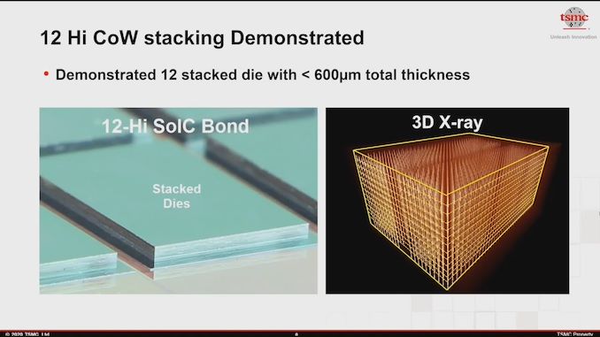
A single slide at the Technology Symposium shows it all off. TMSC is currently probing 12-Hi configurations of SoIC. Each of the dies within the 12-Hi stack has a series of through silicon vias (TSVs) in order for each layer to communicate with the rest of the layers, and the idea is that each layer could be a different element of logic, of IO, of SRAM, or could be passive to act as a thermal insulation layer between other active layers.
This design, as shown in the slide, has a maximum 600 micron thickness according to TSMC, which means that each layer is in the sub-50 micron level. Note that the bump pitch on a standard traditional die-stacking solution can be of the order of 50 microns. In the case of SoIC, the hybrid-bonding pitch is on the scale of 9µm for N7/N6 chips and 6µm for N5 chips. It shows that TSMC has some impressive linear manufacturing and wafer thinning technologies at hand in order to get this level of consistency and aligning of dies. The company has even demonstrated the capability to reduce this down to 0.9µm, a scale at which it would allow it to extend the back-end-of-line interconnect of a silicon chip.
The test chip shown in the slide is likely to be, if it is to showcase some initial runs, only 12 layers of passive silicon with basic TSV management. Obviously building something like this, thermals are going to come into play, but the main aspect here from TSMC’s point of view is that they can build it. It’s now up to the customers to book their place in line for the technology.
Carousel Image from Taiwan Semiconductor Manufacturing Co., Ltd.
Related Reading
- TSMC Details 3nm Process Technology: Full Node Scaling for 2H22 Volume Production
- TSMC To Build 5nm Fab In Arizona, Set To Come Online In 2024
- TSMC & Broadcom Develop 1,700 mm2 CoWoS Interposer: 2X Larger Than Reticles
- TSMC Boosts CapEx by $1 Billion, Expects N5 Node to Be Major Success
- Early TSMC 5nm Test Chip Yields 80%, HVM Coming in H1 2020
- TSMC: 5nm on Track for Q2 2020 HVM, Will Ramp Faster Than 7nm
- TSMC: N7+ EUV Process Technology in High Volume, 6nm (N6) Coming Soon
from AnandTech https://ift.tt/2EqIFyn
via IFTTT
No comments:
Post a Comment